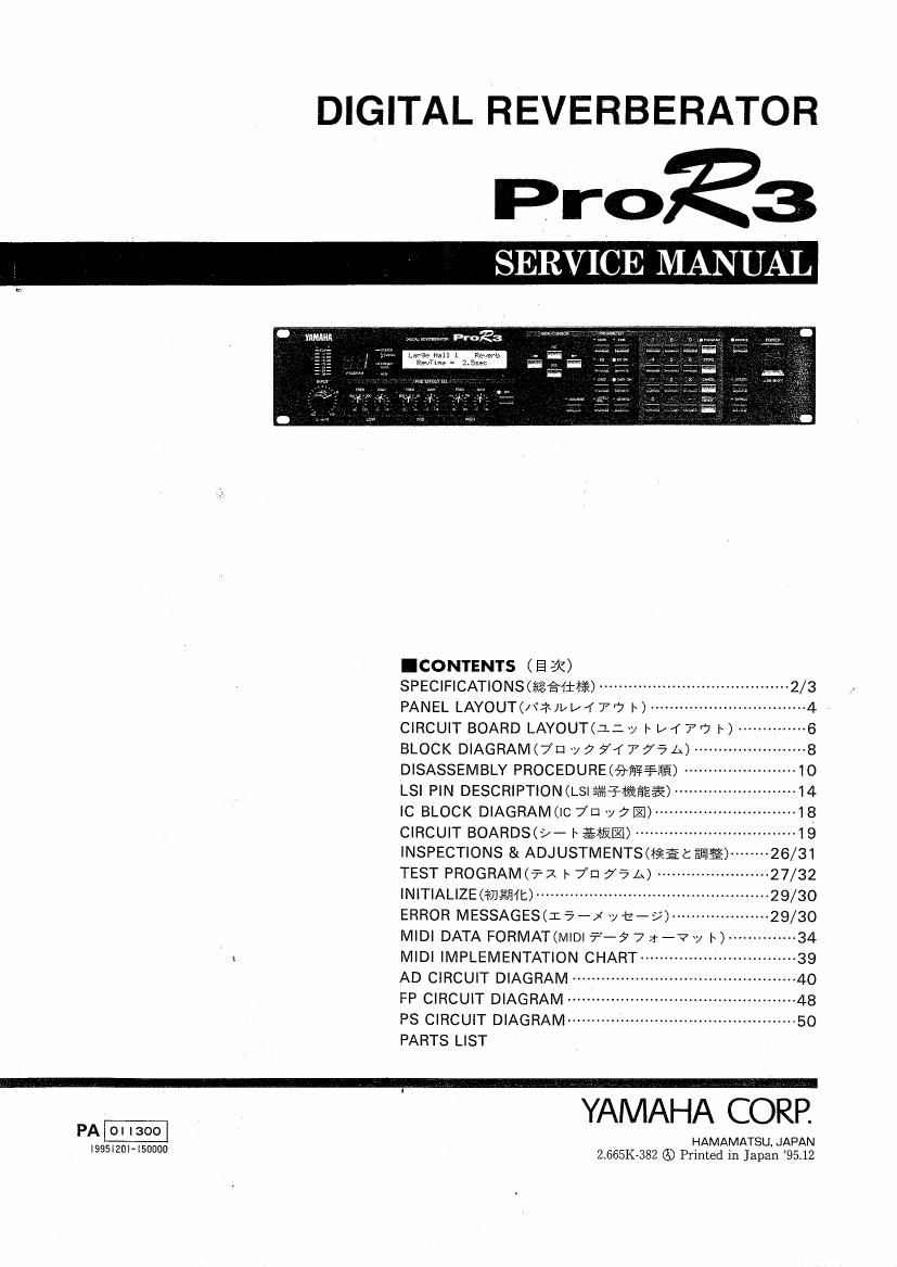
Yamaha pror3 digital reverb service manual

This is the 46 pages manual for yamaha pror3 digital reverb service manual.
Read or download the pdf for free. If you want to contribute, please mail your pdfs to info@audioservicemanuals.com.

Page: 1 / 46
left right
yamaha pror3 digital reverb service manual

Extracted text from yamaha pror3 digital reverb service manual (Ocr-read)


Page 1

DIGITAL REVERBERATOR

Proza

p IIAIIAIIII

.CONTENTS (E 3X)

SPECIFICATIONSOW? Ifléfi) """""""""""""""""""""" 2/3
PANEL LAYOUT(/\$)I,I/4-> I7 I) ................................ 4 .
CIRCUIT BOARD LAYOUTCL: y |~L~r7 r7 |~) ------------ 6
BLOCK DIAGRAM(7D 195747 77A) ----------------------- 8

DISASSEMBLY PROCEDUREIMzIaéIE) ....................... 10
LSI PIN DESCRIPTION IC BLOCK DIAGRAMUC 71: y7i) .48
CIRCUIT BOARDSO- I gym) ~~~~~~~~ .49
INSPECTIONS & ADJUSTMENTSOIfiEt 313%) ~~~~~~~~ 26/31

TEST PROGRAM(7X I7D77A) .... 27/32
INITIALIZEHJJHMB) ------------------------------ 29/30
ERROR MESSAGESIIa x yt- >> -------------------- 29/30
MIDI DATA FORMAT(MIDI -P- 9 7 >r- :7 y I) --»-34

' I MIDI IMPLEMENTATION CHART ------------------- ----39
AD CIRCUIT DIAGRAM ~~~~~~~~~~~~~~~~~~~~ ~~4o
Fp CIRCUIT DIAGRAM ............................................... 48
PS CIRCUIT DIAGRAM ............................................... 50
PARTS LIST

_
YAMAHA CORP.

I
PA HAMAMATSU. JAPAN
I995I2ml50000 2.665K-382 6) Printed in Japan 95.12

Page 2

ProR3

IMPORTANT NOTICE

This manual has been provided for the use of authorized Yamaha Retailers and their service personnel. it has been assumed that basic service
procedures inherent to the industry. and more specifically Yamaha Products. are already known and understood by the users, and have
therefore not been restated.

WARNING: Failure to follow appropriate service and safety procedures when servicing this product may result In personal injury.
destruction of expensive components and failure of the product to perform as specified. For these reasons. we advise
all Yamaha product owners that all service required should be performed by an authorized Yamaha Retailer or the
appointed service representative.

lMPORTANT: The presentation or sale of this manual to any individual or firm does not constitute authorization. certification,
recognition of any applicable technical capabilities, or establish a principal-agent relationship of any form.

The data provided is believed to be accurate and applicable to the unit(s) indicated on the cover. The research, engineering. and service
departments of Yamaha are continually striving to improve Yamaha products. Modifications are. therefore, inevitable and changes in
specification are subject to change without notice or obligation to retrofit. Should any discrepancy appear to exist, please contact the dis-
tributors Service D'wision.

WARNING: Static discharges can destroy expensive components. Discharge any static electricity your body may have
accumulated by grounding yourself to the ground buss In the unit (heavy gauge black wires connect to this buss)

IMPORTANT: Turn the unit OFF during disassembly and parts replacement. Recheck all work before you apply power to the unit.
This product uses a lithium battery for memory back-up.

WARNING: Lithium batteries are dangerous because they can be exploded by improper handling, Observe the following
precautions when handling or replacing lithium batteries.

Leave battery replacement to qualified service personnel.

Always replace with batteries of the same type.

When installing on the PC board. solder using the connection terminals provided on the battery cells.
Never solder directly to the cells. Peifonn the soldering as quickly as possible,

Never reverse the battery polarities when installing.

Do not short the batteries.

Do not attempt to recharge these batteries.

Do not disassemble the batteries.

Never heat batteries or throw them into fire.

ADVARSEL!
Lithiumbatteri. Eksplosionsfare.
Udskiftning ma kun foretages at an sagkyndig, og som beskrevet i servicemanualen.

WARNING: CHEMICAL CONTENT NOTICE!

The solder used in the preduction of this product contains LEAD. in addition, other electrical/electronic and/or plastic (where applicable)
components may also contain traces of chemicals found by the California Health and Welfare Agency (and possibly other entities) to cause
cancer end/or birth defects or other reproductlve ham.

DO NOT PLACE SOLDER. ELECTRICAUELECTRONIC OR PLASTIC COMPONENTS IN YOUR MOUTH FOR ANY REASON
WHAT SO EVER!

Avoid prolonged, unprotected contact between solder and your skinl When soldering. do not inhale solder fumes or expose eyes to solder/flux
vapor!

if you come In contact with solder or components located inside the enclosme of this product, wash your hands before handling food.

I WARNING

Components havlng special characteristics are marked A and must be replaced with parts having specification equal to those
originally installed.

A filmfirfirii. iékifififékbizi¥f;§lfi-'GT. filfi?b$éifl:. aemmafiaemunareerau

Page 14

ProR3

17

0 AK5390-VP (XQ199A00) ADC (Analog Digital Converter)

:15 NAME I/O FUNCTION 52 NAME I/O FUNCTION
1 AGND Analog ground 15 SDATA 0 Serial data output
2 APD I 16 FSYNC |/O Frame synch. clock
3 AIN L+ I Analog signal input (I. channel -) 17 VD+ Digital power supply (+)
4 AINL- 1 Analog signal input (I. channel +) 18 DGND Digital ground
5 ACAL 1 Analog calibration 19 CLK I Master clock
6 LGND Analog logic ground 20 OCLK O 128 15 clock oulput
7 VL+ Analog logic power supply 21 NC
8 NC 22 ICLK I 128 fs clock input
9 DACL 0 Digital calibration 23 VA+ Analog power supply (+)
10 DPD I Digital powar down 24 VA- Analog power supply (-)
11 CMODE l Master clock select 25 AINR- I Analog signal input (R channel -)
(L: CLK=256fs, H:CLK=384fs)
12 SMODE | Interface clock select 26 AINR+ I Analog signal input (R channel +)
(L: slave mode. H: master mode)
13 L/lR |/O Input channel select 27 VREF- 0 Reference voltage (-)
14 SCLK I/O Serial data clock 28 VREF+ 0 Reference voltane (+)
O ADC0809CCN (XG74OAOO) ADC (Analog to Digital Converter)
'23 NAME IIO FUNCTION :13 NAME I/0 FUNCTION
1 1N4 i 15 D2 0 Digital data output
2 INS I 18 VREF(-)
3 INS l Analog input 17 D0 0
4 IN7 I 18 D4 0
5 INS I 19 05 0 Digital data output
6 START l Start data input 20 D6 0
7 E00 0 End of conversion data output 21 D7 0
8 D3 0 Digital data output 22 ALE I Address latch enable
9 OE | Output enable 23 AD2 I
10 CLK | Clock 24 AD1 I } Address data
1 1 VCC Power supply 25 ADD |
12 VREF(+) Reference voltage (+) 26 1N1 I
13 V55 Ground 27 INZ I } Analog input
14 D1 0 Digital data output 28 |N3 l