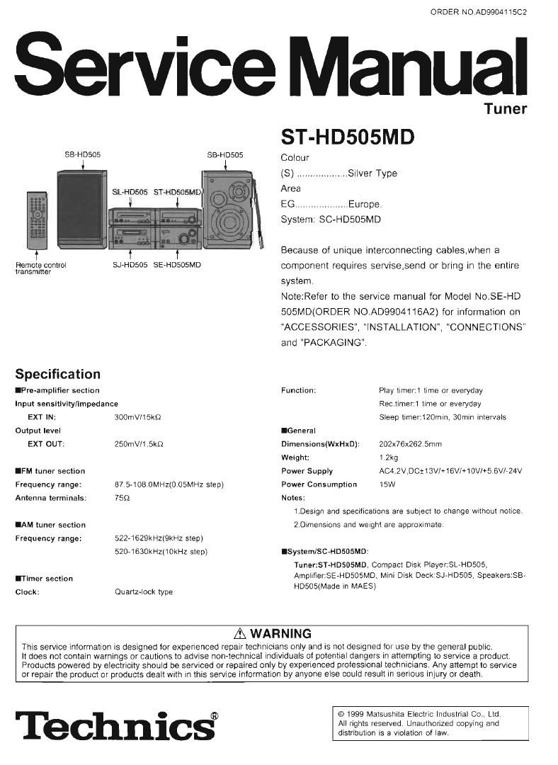
Technics ST HD 505 HD Service Manual

This is the 29 pages manual for Technics ST HD 505 HD Service Manual.
Read or download the pdf for free. If you want to contribute, please mail your pdfs to info@audioservicemanuals.com.

Page: 1 / 29
left right
Technics ST HD 505 HD Service Manual

Extracted text from Technics ST HD 505 HD Service Manual (Ocr-read)


Page 1

ORDER NOADQQOM 1502

Service Manual

SB-HDSOS

l I SL'HDSOS ST-HDSOSMD

Remote control
transmitter

Specmcafion

IPre-amplifier section

S B-HDSOS

t

SJ-HD505 SE-HDSOSMD

Input sensitivity/impedance

EXT IN:
Output level
EXT OUT:

IFM tuner section
Frequency range:
Antenna terminals:

IAM tuner section

Frequency range:

[Timer section
Clock:

300mV/15kQ

250mV/1.5kQ

87.5-108 OMHZ(0.05MH2 step)
75:2

52271629kHz(9kHz step)
520-1630kHzt10kHz step)

Quartz-lock type

Tuner

ST-HD505MD

Colour

(8) ................... Silver Type
Area

EG .................... Europe.

System: SC-HDSOSMD

Because of unique interconnecting cableswhen a
component requires servise,send or bring in the entire
system,

NotezRefer to the sen/ice manual for Model No.SE-HD
505MD(ORDER NO.AD9904116A2) tor information on
ACCESSORIES, INSTALLATION", CONNECTIONS"
and "PACKAGING.

Function; Play llll'lelil lime or everyday
Rec.timer:1 time or everyday
Sleep timerzt20min, 30min intervals

IGeneral

DimensionsMxHxD): 202x76x262 5mm

Weight: 1 2kg

Power Supply ACA.2V,DC:13V]+16V/+10V/+5.6V/-24V
Power Consumption 15W

Notes:

1.DeSi9n and specifications are subject to change Without notice.
2Dimensions and weight are approximate,

lSystem/SC-HDSOSMD:
Tuner:ST-HD§05MD, Compact Disk PlayerJSL-HDSOE),
AmplifierzSErHDSOSMD. Mini Disk Deck SJ-HDSOS, SpeakerSJSB-
HD505(Made in MAES)

A WARNING

This service information is designed tor experienced repair technicians only and is not deSigned for use by the general public.

It does not contain warnings or cautions to adVise nonitechnical indIVIduals of potential dangers in attempting to service a product.
Products powered by electricity should be serviced or repaired only by experienced professional technicians. Any attempt to service
or repair the product or products dealt With in this sen/ice intormation by anyone else could result in serious injury or death.

Technics®

© 1999 Matsushita Electric Industrial Co., Ltd.
All rights reserved Unauthorized copying and
distribution is a Violation of law.

Page 2

ST-HDSDEMD

7CONTENTS

1 Before Repair ------------------------------------------


2 Blue LED rrrrrrrrrrrrrrrrrr

3 Operating Instructions-

4 About the Self-Diagnostic Mode --------------------------------------------- 5
5 Power Source ONIOFF and Signal Check ----------------------------- 6
6 Operation Checks and Component Replacement Procedures-7

7 Wiring Connection Diagram-

8 Block Diagram
12

9 Schematic Diagram Notes
9.1. Schematic Diagram Notes ''''''''''''''''''''''''''''''''''' 12

1 Before Repair

This equipment (ST-HD505MD). which is a component of the
system, is supplied with power from the amplifier (SE7
HDSOSMD).When repairing this equipment or checking

2 Blue LED

Page

9.2. Type Illustration of lC's Transistors and Diodes ------------- 12

>13

11 Printed Circuit Board Diagram -20

12 Terminal Function of lC's ----------------------------------------------------- 24

12.1, |0302(M62433AFP): DIGITAL SOUND CONTROLLER-24
12.2, |C701(M30218MAA101): FL DRIVE/SYSTEM CONTROL

1!) Schematic Diagram m...

~25
13 Replacement Parts List 26
14 Cabinet Parts Location ----------------------------------------------------- 29

operation of the system, be sure to connect the amplifier with it.

Power supply and operation check in the state of it as a single
equipmenet are impracticable.

. The LED mounted to each side of the front panel of this set is very sensitive to static electricitywrien handling the LED base

plate, be very careful about it.

9 Do not replace a blue LED singly. If replaced singly, it may be subject to electrostatic breakdown or deterioration in quality,
When replacing the LED base plate, be sure to replace L and R sides simuitaneously to permit the brightness adjustment.

For configuration at the time of supply of replacement parts, refer to Printed Circuit Board Diagram.

Page 24

STVH DSOEMD

12 Terminal Function of lCs
12.1. |C302(M62433AFP): DIGITAL SOUND CONTROLLER

Pin Mark [)0 Function Pin Mark IIO Function
No. Division No. Division
1 PSelN O R/L output terminal for surround 40 882 I Bass boost capacity connection
2 PS+IN I Phase shift filter lnput terminal for terminaI(N0t 53¢ 509519d 0
surround (Not used, open) GND)
3 K|N1 0 Key control adaptor output terminal 41 VOLOUTZ O R ladder volume output terminal
(Not used, open) 42 VOLIN2 I R ladder volume input terminal
4 KOUT1 1 Key control adaptor input terminal 43 GEQOUT2 0 Tone signal output termlnal
(N01 USSUI connected 0 GND) 44 F5F2 | Band pass filter connect termlnal
5 TAPERECi O Rec signal output terminal from (Connected to GND through
surround mix amp. terminal capacitor)
6 MDRECi 0 Select common output rec Signal 45 F4lN2 l Resonance buffer amp input terminal
7 EXT OUT1 0U1DUI terminal 46 F402 0 Resonance buffer amp output
8 DPLt I Tone signal input terminal (Not used. terminal
connected to GND) 47 F4F2 I Resonance impedance connect
9 F1F1 | Resonance impedance connect terminal
terminal 48 F3lN2 | Resonance buffer amp input terminal
10 F101 0 Resonance buffer amp output 49 F302 0 Resonance buffer amp output
terminal termlnal
11 F|N1 | Resonance buffer amp input terminal 50 F3F2 l Resonance impedance connect
12 F2F1 l Resonance impedance connect terminal
terminal 51 F2IN2 l Resonance buffer amp input terminal
13 F201 0 Resonance buffer amp output 52 F202 0 Resonance buffer amp output
terminal terminal
14 F2|N1 l Resonance buffer amp input terminal 53 FZFZ I Resonance impedance connect
15 F3F1 l Resonance impedance connect terminal
terminal 54 F1IN2 I Resonance buffer amp input terminal
16 F301 0 Resonance buffer amp output 55 F102 0 Resonance buffer amp output
terminal terminal
17 Palm l Resonance buffer amp input terminal 56 F1F2 l Resonance impedance connect
18 F4F1 I Resonance impedance connect terminal
terminal 57 DPLZ I Tone signal input terminal
19 F401 0 Resonance buffer amp output (NOI used. connected 0 GND)
terminal 58 EXT OUTZ 0 Select common output rec signal
20 Him I Resonance buffer amp input terminal 59 MD RECZ 0 °U1PUt terminal
21 F5F1 | Band pass filter connect terminal 50 TAPE 0 Rec signal output terminal from
(Connected to GND through RECZ surround mix amp. terminal
capacitor) 61 MIC IN I Mic signal input terminal
22 GEOOUTi 0 Tone signal output terminal (Not used. connected to GND)
23 VOLlN1 I R ladder volume input terminal 62 KOUT2 | Key control adaptor input terminal
24 VOLOUT1 o R ladder volume output terminal (Not usedi connected to GND)
25 BB1 _ Bass boost capacity connection 63 KIN2 0 Key control adaptor output terminal
terminal(Not used connected to (Not USEdi open)
GND) 64 BPOUT 0 Band pass filler amp output terminal
26 BUFIN I Bass boost amp (+) input terminal for vocal cancel
27 BUFNF1 | Bass boost amp l-J input terminal 55 BPIN | Band pass filter amp input terminal
28 BUFOUT1 0 Bass boost amp output terminal for vocal cancel
29 PORTA o For! A output terminal (Not used 56 CD ' npu emlna f°r RC
open) 67 TUNER
30 PORTB 0 Port B output terminal 68 MD
31 DVDD | Power supply terminal 59 TAPE
32 CLK | Clock input terminal for serial data 70 AUXH
transfer 71 AUXL
33 DATA l Control data input terminal 72 AVSS | Power supply terminal
34 LATCH | Latch signal input terminal 73 AGND - GND terminal
35 DGND - GND terminal 74 AUXL | Input terminal for Lch
36 AVDD I Power supply terminal 75 AUXH
37 BUFOUT2 0 Bass boost amp output terminal 76 TAPE
38 BUFNFZ | Bass boost amp t») input terminal 77 MD
39 BUFIN2 | Bass boost amp (+) input terminal 73 TUNER
79 CD
80 DELIN R/l. input terminal for surround

24