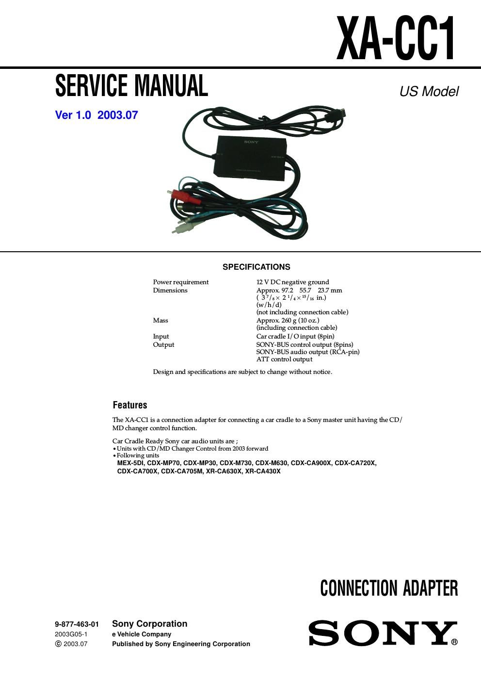
Page 1
2
XA-CC1
1. GENERAL ................................................................... 3
2. DIAGRAMS ................................................................. 4
2-1. Note for Printed Wiring Boards and Schematic Diagram ......................................................... 4
2-2. Schematic Diagram ......................................................... 5
2-3. Printed Wiring Board -“ BUS Board (Component Side) -“ ................................. 6
2-4. Printed Wiring Board -“ BUS Board (Conductor Side) -“ ................................... 7
2-5. IC Pin Function Description........................................... 8
3. EXPLODED VIEW ................................................... 9
4. ELECTRICAL PARTS LIST ............................... 10
TABLE OF CONTENTS Notes on chip component replacement
-N ever reuse a disconnected chip component.
- Notice that the minus side of a tantalum capacitor may be dam-
aged by heat.
UNLEADED SOLDER
Boards requiring use of unleaded solder are printed with the lead-
free mark (LF) indicating the solder contains no lead.
(Caution: Some printed circuit boards may not come printed with the lead free mark due to their particular size)
: LEAD FREE MARK
Unleaded solder has the following characteristics.
- Unleaded solder melts at a temperature about 40 ËšC higher than
ordinary solder.
Ordinary soldering irons can be used but the iron tip has to be
applied to the solder joint for a slightly longer time.
Soldering irons using a temperature regulator should be set to
about 350 ËšC.
Caution: The printed pattern (copper foil) may peel away if the
heated tip is applied for too long, so be careful!
- Strong viscosity
Unleaded solder is more viscou-s (sticky, less prone to flow)
than ordinary solder so use caution not to let solder bridges oc-
cur such as on IC pins, etc.
- Usable with ordinary solder
It is best to use only unleaded solder but unleaded solder may
also be added to ordinary solder.