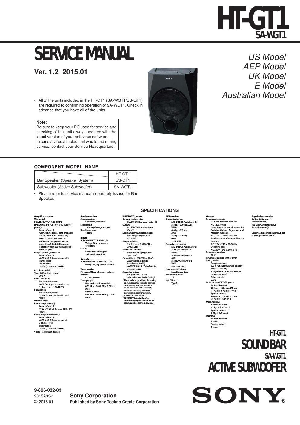
Page 1
HT-GT1
2
NOTES ON CHIP COMPONENT REPLACEMENT
- Never reuse a disconnected chip component.
- Notice that the minus side of a tantalum capacitor may be dam-aged by heat.
License and Trademark Notice
MPEG Layer-3 audio coding
technology and patents licensed
from Fraunhofer IIS and Thomson.
Windows Media is either a registered trademark or trademark
of Microsoft Corporation in
the United States and/or other
countries.
This product is protected by certain intellectual property rights
of Microsoft Corporation. Use or
distribution of such technology
outside of this product is prohibited
without a license from Microsoft or
an authorized Microsoft subsidiary.
The BLUETOOTH® word mark and logos are registered trademarks
owned by Bluetooth SIG, Inc. and
any use of such marks by Sony
Corporation is under license. Other
trademarks and trade names are
those of their respective owners.
The N Mark is a trademark or registered trademark of NFC Forum,
Inc. in the United States and in other
countries.
Android-„¢ is a trademark of Google Inc.
Google Play-„¢ is a trademark of Google Inc.
iPhone and iPod touch are trademarks of Apple Inc., registered
in the U.S. and other countries. App
Store is a service mark of Apple Inc.
Made for iPod and Made for iPhone mean that an electronic
accessory has been designed
to connect specifically to iPod
or iPhone, respectively, and has
been certified by the developer
to meet Apple performance
standards. Apple is not responsible for the operation of this device
or its compliance with safety and
regulatory standards. Please note
that the use of this accessory with
iPod or iPhone may affect wireless
performance.
All other trademarks and registered trademarks are of their respective
holders. In this manual, -„¢ and ®
marks are not specified.
SAFETY-RELATED COMPONENT WARNING!
COMPONENTS IDENTIFIED BY MARK 0 OR DOTTED LINE
WITH MARK 0 ON THE SCHEMATIC DIAGRAMS AND IN
THE PARTS LIST ARE CRITICAL TO SAFE OPERATION.
REPLACE THESE COMPONENTS WITH SONY PARTS
WHOSE PART NUMBERS APPEAR AS SHOWN IN THIS
MANUAL OR IN SUPPLEMENTS PUBLISHED BY SONY.
Ve r. 1 . 1
SAFETY CHECK-OUT
After correcting the original service problem, perform the follow-
ing safety check before releasing the set to the customer:
Check the antenna terminals, metal trim, metallized knobs,
screws, and all other exposed metal parts for AC leakage.
Check leakage as described below.
LEAKAGE TEST
The AC leakage from any exposed metal part to earth ground and
from all exposed metal parts to any exposed metal part having a
return to chassis, must not exceed 0.5 mA (500 microamperes.).
Leakage current can be measured by any one of three methods.
1. A commercial leakage tester, such as the Simpson 229 or RCA WT-540A. Follow the manufacturers instructions to use these
instruments.
2. A battery-operated AC milliammeter. The Data Precision 245 digital multimeter is suitable for this job.
3. Measuring the voltage drop across a resistor by means of a VOM or battery-operated AC voltmeter. The limit indication
is 0.75 V, so analog meters must have an accurate low-voltage
scale. The Simpson 250 and Sanwa SH-63Trd are examples
of a passive VOM that is suitable. Nearly all battery operated
digital multimeters that have a 2 V AC range are suitable. (See
Fig. A)
1.5 kΩ
0.15 μF AC
voltmeter
(0.75 V)
To Exposed Metal
Parts on Set
Earth Ground
Fig. A. Using an AC voltmeter to check AC leakage.
Page 2
HT-GT1
3
1. SERVICING NOTES ............................................. 4
2. DISASSEMBLY
2-1. Disassembly Flow ........................................................... 6
2-2. Side L, R Panel ............................................................... 7
2-3. Top Panel Block .............................................................. 8
2-4. Front Panel Block ........................................................... 9
2-5. NFC Module (NFC1) ...................................................... 10
2-6. Bluetooth Module (BT1) ................................................ 11
2-7. PANEL Board Block ....................................................... 12
2-8. Button Assy ..................................................................... 13
2-9. Knob Assy ....................................................................... 14
2-10. Top Panel Assy ................................................................ 15
2-11. Rear Panel Block ............................................................ 16
2-12. DC Fan (M1) ................................................................... 17
2-13. TUNER Board ................................................................ 17
2-14. MAIN Board-1 ................................................................ 18
2-15. MAIN Board-2 ................................................................ 19
2-16. Sub Chassis ..................................................................... 20
2-17. Power Cord (AC1) .......................................................... 21
2-18. SMPS Board ................................................................... 22
2-19. Loudspeaker (18 cm) (SP1) ............................................ 23
2-20. Service Position .............................................................. 24
3. TEST MODE ............................................................ 25
4. ELECTRICAL CHECK ......................................... 27
5. TROUBLESHOOTING .......................................... 28
TABLE OF CONTENTS6. DIAGRAMS
6-1. Block Diagram - MAIN Section - ................................... 29
6-2. Block Diagram - AMP Section - ..................................... 30
6-3. Block Diagram - PANEL/POWER SUPPLY Section - ............................ 31
6-4. Schematic Diagram - MAIN Section (1/5) - ................... 33
6-5. Schematic Diagram - MAIN Section (2/5) - ................... 34
6-6. Schematic Diagram - MAIN Section (3/5) - ................... 35
6-7. Schematic Diagram - MAIN Section (4/5) - ................... 36
6-8. Schematic Diagram - MAIN Section (5/5) - ................... 37
6-9. Printed Wiring Boards - MAIN Section (1/2) - .............. 38
6-10. Printed Wiring Board - MAIN Section (2/2) - ................ 39
6-11. Printed Wiring Boards - KEY Section - .......................... 40
6-12. Schematic Diagram - KEY Section - .............................. 41
6-13. Printed Wiring Board - PANEL Board - ......................... 42
6-14. Schematic Diagram - PANEL Board - ............................ 43
6-15. Printed Wiring Board - SMPS Board - ........................... 44
6-16. Schematic Diagram - SMPS Board - .............................. 45
7. EXPLODED VIEWS
7-1. Side Panel Section .......................................................... 53
7-2. Top Panel Section ........................................................... 54
7-3. Front Panel Section ......................................................... 55
7-4. MAIN Board Section ...................................................... 56
7-5. SMPS Board Section ...................................................... 57
7-6. Speaker Cabinet Section ................................................. 58
8. ELECTRICAL PARTS LIST .............................. 59
Accessories are given in the last of the electrical parts list.