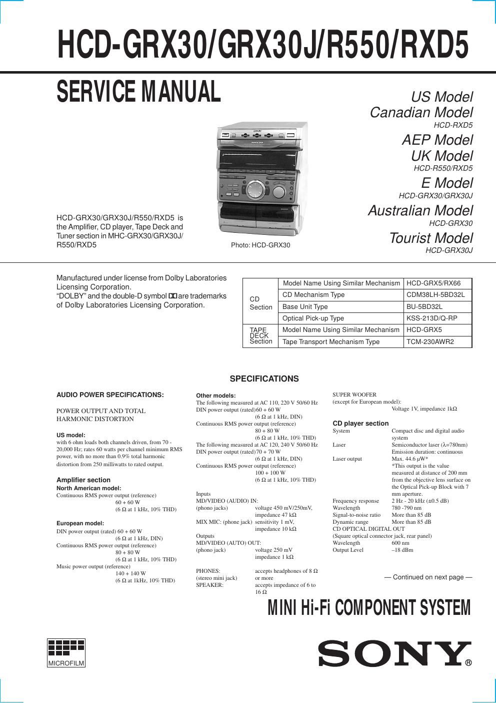
Sony hcd grx 30 grx 30j r550 rxd5

This is the 68 pages manual for sony hcd grx 30 grx 30j r550 rxd5.
Read or download the pdf for free. If you want to contribute, please mail your pdfs to info@audioservicemanuals.com.

Page: 1 / 68
left right
sony hcd grx 30 grx 30j r550 rxd5

Extracted text from sony hcd grx 30 grx 30j r550 rxd5 (Ocr-read)


Page 1

Ñ 2 Ñ Tape player sectionRecording system 4-track 2-channel stereo Frequency response 40 - 13,000 Hz (±3 dB), (DOLBY NR OFF) using Sony TYPE I cassette 40 - 14,000 Hz (±3 dB), using Sony TYPE II cassette Tuner sectionFM stereo, FM/AM superheterodyne tuner FM tuner sectionTuning range 87.5 - 108.0 MHz Antenna FM lead antenna Antenna terminals 75 W unbalanced Intermediate frequency 10.7 MHz AM tuner sectionTuning range 2 Band type: North American models: 530 - 1,710 kHz (with the interval set at 10 kHz) 531 - 1,710 kHz (with the interval set at 9 kHz) European model: 531 Ð 1,602 kHz (with the interval set at 9 kHz) Other models: 531 - 1,602 kHz (with the interval set at 9 kHz) 530 - 1,710 kHz (with the interval set at 10 kHz) 3 Band type: Middle Eastern model: MW: 531 Ð 1,602 kHz (with the interval set at 9 kHz) SW: 5.95 Ð 17.90 MHz (with the interval set at 5 kHz) Other models: MW: 531 Ð 1,602 kHz (with the interval set at 9 kHz) 530 Ð 1,710 kHz (with the interval set at 10 kHz) SW: 5.95 Ð 1,790 kHz (with the interval set at 5 kHz) Antenna AM loop antenna Antenna terminals External antenna terminal Intermediate frequency 450 kHz GeneralPower requirements North American model: 120 V AC, 60 Hz European model: 230 V AC, 50/60Hz Australian model: 230 Ð 240 V AC, 50/60 Hz Mexican model: 120 V AC, 50/60 Hz Thailand model: 220 - 240 V AC, 50/60 Hz Other models: 110 - 120 V or 220 - 240 V AC, 50/60 Hz Power consumption U.S.A. model: 130 W Canadian model: 110 W East European model: 130W Other models: 110 W Dimensions (w/h/d) Approx. 280 ´ 340 ´ 380 mm (11 ´ 13 3/8 ´ 15 in.) Mass: Approx. 9.5 kg (21 lb.) Supplied accessories: AM loop antenna (1) Remote commander (1) Batteries (2) FM lead antenna (1) Speaker cords (2) (for European model only) Design and specifications are subject to change without notice.

Page 2

Ñ 3 Ñ SECTION 1 SERVICING NOTES The laser diode in the optical pick-up block may suffer electrostatic break-down because of the potential difference generated by the charged electrostatic load, etc. on clothing and the human body. During repair, pay attention to electrostatic break-down and also use the procedure in the printed matter which is included in the repair parts. The flexible board is easily damaged and should be handled with care. NOTES ON LASER DIODE EMISSION CHECK The laser beam on this model is concentrated so as to be focused on the disc reflective surface by the objective lens in the optical pick- up block. Therefore, when checking the laser diode emission, observe from more than 30 cm away from the objective lens. Notes on chip component replacement ¥ Never reuse a disconnected chip component. ¥ Notice that the minus side of a tantalum capacitor may be dam- aged by heat. Flexible Circuit Board Repairing ¥ Keep the temperature of the soldering iron around 270 ûC dur- ing repairing. ¥ Do not touch the soldering iron on the same conductor of the circuit board (within 3 times). ¥ Be careful not to apply force on the conductor when soldering or unsoldering. NOTES ON HANDLING THE OPTICAL PICK-UP BLOCK OR BASE UNIT CAUTION Use of controls or adjustments or performance of procedures other than those specified herein may result in hazardous radiation exposure. This appliance is classified as a CLASS 1 LASER product. The CLASS 1 LASER PRODUCT MARKING is located on the rear exterior. Laser component in this product is capable of emitting radiation exceeding the limit for Class 1. The following caution label is located inside the unit. 1. SERVICING NOTES ááááááááááááááááááááááááááááááááááááááááááááááááááá\ 3 2. GENERAL ááááááááááááááááááááááááááááááááááááááááááááááááááá\ ááááááááááááááááááá 6 3. DISASSEMBLY 3-1. Case ááááááááááááááááááááááááááááááááááááááááááááááááááá\ ááááááááááááááááááááááááááááááááá 8 3-2. Front Panel Section ááááááááááááááááááááááááááááááááááááááááááááááááááá\ ááááááááá 8 3-3. Tape Mechanism Deck Section (TCM-230AWR2) áááááááááááá 9 3-4. CD Mechanism Deck section (CDM38LH-5BD32L) áááááááá 9 3-5. Main Board ááááááááááááááááááááááááááááááááááááááááááááááááááá\ áááááááááááááááááááá 10 4. TEST MODE ááááááááááááááááááááááááááááááááááááááááááááááááááá\ ááááááááááááá 11 5. MECHANICAL ADJUSTMENTS áááááááááááááááááááááááááá 13 6. ELECTRICAL ADJUSTMENTS ááááááááááááááááááááááááááá 13 7. DIAGRAMS 7-1. Circrit Boards Location ááááááááááááááááááááááááááááááááááááááááááááááááááá\ á 18 7-2. Block Diagrams ááááááááááááááááááááááááááááááááááááááááááááááááááá\ ááááááááááááá 19 · CD Section ááááááááááááááááááááááááááááááááááááááááááááááááááá\ áááááááááááááááááá 19 · Tape Deck Section ááááááááááááááááááááááááááááááááááááááááááááááááááá\ áááááá 21 · Main Section ááááááááááááááááááááááááááááááááááááááááááááááááááá\ ááááááááááááááá 23 · Display/Key Con Section áááááááááááááááááááááááááááááááááááááááááááááá 25 7-3. Printed Wiring Board Ð CD Section Ð áááááááááááááááááááááááááááááá 29 7-4. Schematic Diagram ÐCD Section Ð áááááááááááááááááááááááááááááááááá 31 7-5. Printed Wiring Board Ð CD Motor Section Ð ááááááááááááááááááá 33 7-6. Schematic Diagram Ð CD Motor Section Ð áááááááááááááááááááááá 35 7-7. Printed Wirint Board Ð Tape Deck Section Ð ááááááááááááááááááá 37 7-8. Schematic Diagram Ð Tape Deck Section Ð ááááááááááááááááááááá 39 7-9. Printed Wiring Board Ð Leaf SW Section Ð ááááááááááááááááááááá 41 7-10. Schematic Diagram Ð Leaf SW Section Ð áááááááááááááááááááááááá 42 7-11. Printed Wiring Board Ð Main Section Ð ááááááááááááááááááááááááááá 43 7-12. Schematic Diagram Ð Main Section (1/4) Ð ááááááááááááááááááááá 45 7-13. Schematic Diagram Ð Main Section (2/4) Ð ááááááááááááááááááááá 47 7-14. Schematic Diagram Ð Main Section (3/4) Ð ááááááááááááááááááááá 49 7-15. Schematic Diagram Ð Main Section (4/4) Ð ááááááááááááááááááááá 51 7-16. Printed Wiring Board Ð Panel Section Ð ááááááááááááááááááááááááááá 53 7-17. Schematic Diagram Ð Panel Section Ð ááááááááááááááááááááááááááááá 55 7-18. Printed Wiring Board Ð AC Sec Standby Section Ð áááááááááá 57 7-19. Schematic Diagram Ð AC Sec Standby Section Ð áááááááááááá 59 7-20. Printed Wiring Board Ð CD SW Section Ð ááááááááááááááááááááááá 61 7-21. Schematic Diagram Ð CD SW Section Ð áááááááááááááááááááááááááá 61 7-22. IC Block Diagrams ááááááááááááááááááááááááááááááááááááááááááááááááááá\ áááááááá 63 7-23. IC PIN Function Description áááááááááááááááááááááááááááááááááááááááááááá 66 8. EXPLODED VIEWS 8-1. Case Section ááááááááááááááááááááááááááááááááááááááááááááááááááá\ áááááááááááááááááá 69 8-2. Front Panel Section ááááááááááááááááááááááááááááááááááááááááááááááááááá\ ááááááá 70 8-3. Chassis Section ááááááááááááááááááááááááááááááááááááááááááááááááááá\ áááááááááááááá 71 8-4. CD Mechanism Deck Section-1 (CDM38LH-5BD32L) áá 73 8-5. CD Mechanism Deck Section-2 (CDM38LH-5BD32L) áá 74 8-6. Base Unit Section (BU-5BD32L) ááááááááááááááááááááááááááááááááááááá 75 8-7. Tape Mechanism Deck Section-1 (TCM-230AWR2) áááááá 76 8-8. Tape Mechanism Deck Section-2 (TCM-230AWR2) áááááá 77 9. ELECTRICAL PARTS LIST ááááááááááááááááááááááááááááááááááá 78 TABLE OF CONTENTS