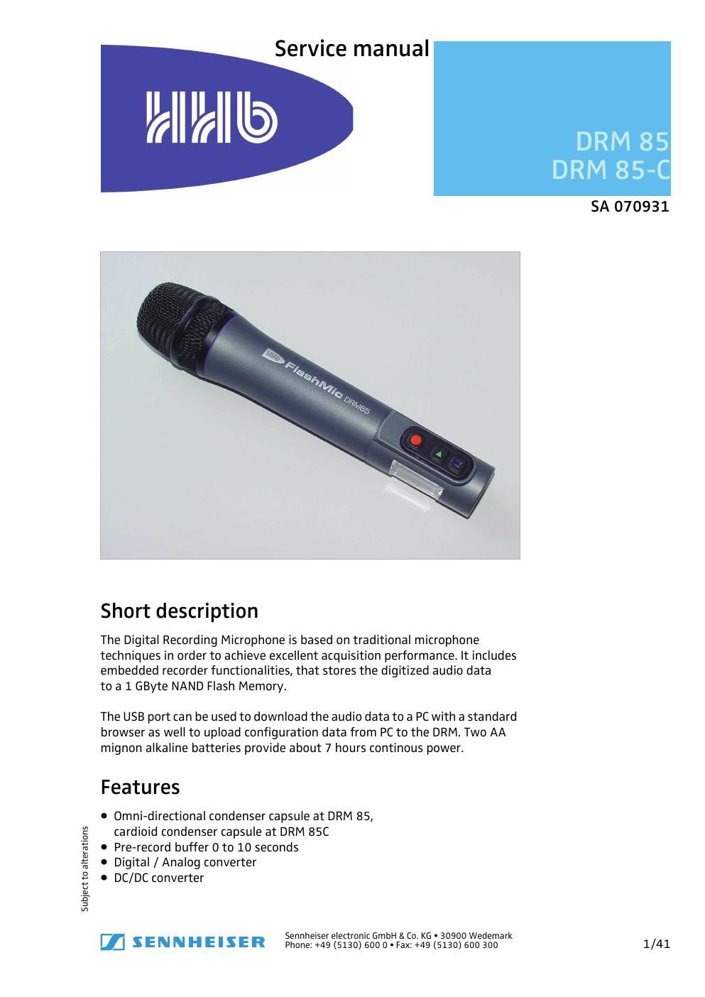
Sennheiser drm 85 85c digital recording mic service manual

This is the 41 pages manual for sennheiser drm 85 85c digital recording mic service manual.
Read or download the pdf for free. If you want to contribute, please mail your pdfs to info@audioservicemanuals.com.

Page: 1 / 41
left right
sennheiser drm 85 85c digital recording mic service manual

Extracted text from sennheiser drm 85 85c digital recording mic service manual (Ocr-read)


Page 1

DRM 85-C, DRM 85 2/4109/2007 Safety requirements Observe safety regulations. Observe ESD instructions while handling electrostatically endangered components. Only skilled persons are allowed to alter and repair. For repairs and exchanges only approved components according to the current spare parts list are allowed. For safety and certification reasons it is forbidden to alter the product without authorization. Otherwise, the person who has altered the product is liable for any consequential damage. repairs/exchangesThe following instructions for overhaul and testing must be followed. In case of unusual problems please contact your Sennheiser distributor. CAUTION During SMD component soldering you may destroy them by using a standard soldering iron for several seconds. Only use adapted soldering tools when soldering SMD components. SMD

Page 2

DRM 85-C, DRM 85 09/20073/41 Contents 1 Controls and indicators.................................................................................. 4 2 Specifications .................................................................................................. 5 3 Description ...................................................................................................... 7 3.1 Mechanical design ................................................................................................ 7 3.2 Electrical design .................................................................................................... 7 3.3 Functional description ......................................................................................... 7 3.4 Disassembly ......................................................................................................... 14 3.5 Assembly .............................................................................................................. 21 3.6 Firmware including updates ............................................................................. 24 3.7 Known faults ....................................................................................................... 25 4 Exploded view .............................................................................................. 26 5 Test and alignment instructions ............................................................... 28 5.1 Measuring set-up................................................................................................ 28 5.2 Test table ............................................................................................................. 29 6 Circuit diagrams ........................................................................................... 31 Block diagram ...................................................................................................................31 AF board, circuit diagram ............................................................................................... 32 AF board, printed circuit board, component side ...................................................... 33 AF board, printed circuit board, solder side................................................................ 33 Connector board, circuit diagram ................................................................................. 34 Connector board, printed circuit board, solder side .................................................. 35 Connector board, printed circuit board, component side ........................................ 35 Keyboard PCB, circuit diagram ...................................................................................... 36 Keyboard PCB, printed circuit board, component side ............................................. 36 Keyboard PCB, printed circuit board, solder side ....................................................... 36 Processor board, circuit diagram, part 1/3 ................................................................. 37 Processor board, circuit diagram, part 2/3 ................................................................. 38 Processor board, circuit diagram, part 3/3 ................................................................. 39 Processor board, printed circuit board, component side ......................................... 40 Processor board, printed circuit board, solder side ................................................... 41