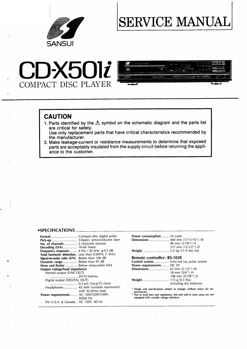
Sansui CD X501I Service Manual

This is the 18 pages manual for Sansui CD X501I Service Manual.
Read or download the pdf for free. If you want to contribute, please mail your pdfs to info@audioservicemanuals.com.

Page: 1 / 18
left right
Sansui CD X501I Service Manual

Extracted text from Sansui CD X501I Service Manual (Ocr-read)


Page 1

ISERVICE MANUAL

SANSUI

CD-X50li

COMPACT DISC PLAYER

CAUTION

are critical for safety.

the manufacturer.

ance to the customer.

1. Parts identified by the A symbol on the schematic diagram and the pans list
Use only replacement parts that have critical characteristics recommended by

2. Make leakage-current or resistance measurements to determine that exposed
pans are acceptably insulated from the supply circuit before returning the appli-

SPECIFICATIONS

FormaL .. Compact disc digital audio
3»beam, semiconductor laser
2 channels (stereol
Decoding (D/A)..167bit linear
Frequency response 4 Hz~20 kHz *0.3 dB
Total harmonic distortion. Less than 0.003% (1 kHz)
Signal- to-noise ratio (S/N)'. Better than 106 dB
Dynamic range... Better than 97 dB
Wow and flutter. Below measurable limit
Output voltage/load impedance

Normal output (LlNE OUT)

............................. ZVIIO kohms

Digital output (DIGITAL OUT)
.0 5:1:0.1Vp p175 ohms
45 mW (variable maximum)/
with 32-ohrns load
Power requirements ........ AC 120V/220V/240V,

50/60 HZ
For U.S.A. 8r Canada .. AC 120V, 60 HZ

Headphone

Power consumption .. 16 watts
Dimensions.. .. 448 mm (17-11/16) W
98 mm (3-7/8) H
317 mm (12-1/2) D
Weight ............................ 5.4 kg (11.9 lbs) net

Remote controller: RS- 1020
Control system ....... .l-nfra red ray pulse system
Power requirements DC 3V
Dimensions: ........ .. 63 mm (ZAi/Z") W

18 mm (3/4 ) H

148 mm (5-7/8) D
Weight ............................ 115 g (03 lbs)

including dry batteries

- Design and specifications subject In changes without notice tor im~
movements.

- Due to local laws and regulations, this unit sold in some areas are m
equipped with variable voltage selecltors.

Page 2

1. The symbols, UL, CSA, SA, BS, UK, EU, AS, SEV, SS and
XX < EXPORT> on the parts list and the schematic dia-
gram mean followings respectively.

UL ...................... Manufactured for U.S.A market.
(Underwriters Laboratories approved
model.)

CSA . Manufactured for Canadian market.

SA... . Manufactured for South African market.

BS, UK ............... Manufactured for United Kingdom
market.

. Manufactured for European market.

. Manufactured for Australian market.

. Manufactured for Swiss market.

. Manufactured for Saudi Arabia market.
. Standard Version.

XX...

NON MARK ........ Common Parts.

. 2. Some printed circuit boards are not supplied assembled.

To separate these in this service manual, the stock num-
bers are not indicated for these boards. However, stock
numbers for individual parts are indicated.

3. Since some capacitors and resistors are omitted from pans
lists in this service manual, refer to the Common Parts List
for capacitors and resistors, which was issued on June
1987.

NOTE

4. Abbreviations in this service manual are as follows.

- OAbbreviations List

CR : Carbon Resistor

S.R. : Solid Resistor

CeR. : Cement Resistor

MR : Metal Film Resistor

F.R. : Fusing Resistor

N.|.R. : Non-inflammable Resistor

A.R. : Array Resistor

CC. : Ceramic Capacitor

C.T. : Ceramic Capacitor, Temperature
Compensation

EC. : Electrolytic Capacitor

E.L. : Low Leak Electrolytic Capacitor

E.B. : Bi-Polar Electrolytic Capacitor

E.B.L. : Low Leak Bi-Polar Electrolytic
Capacitor

Tac. : Tantalum Capacitor

F.C. : Film Capacitor

MP. : Metalized Paper Capacitor

PC : Polystyrene Capacitor

M.M.C : Metaliied Mylar Capacitor
AC. : Array Capacitor

V.R. : Variable Resistor

S.V.R. : Semi Variable Resistor
SW : Switch

Chip R. : Chip Resistor
Chip C. : Chip Capacitor

Cautions Concerning Handling of The Laser

The following lable has been alfixed to the unit, listing the proper procedure for

working with the laser beam.


ieu modal mm

(UL Ind xx model onlyt

waonucr couvtles wim anus
nutzs 2r cm suacuAPrER J
mar mu to

minimum

tcSA moat only)
csnnnan on To mww
ammo». coo:

CERYlFlE EN VERTU cu CODE
comm a: L'ELECTRiCrrE
ssutzusm

[EU model only)


CLASS 1
LASER PRODUCY

Page 5

CDX50H

oCXA1082AS (Servo Control)

CLV LPF
vco FlL

3.5V nEeuLnoR

11L DATA IEstYER luPur SHlFT REGISTER
ADDRESS DECODER
sEquncER

outrur oEcocER

FSI~4 TGI~Z TMl-I

ii

m5
coup: NSATION

|____

\vt
CMMATOI

Focus PHASE
COMPARATOR

n:

i \H.

o-u

0 Terminal Function

Pin No. Pin Name IIO Description Pin No. Pin Name IIO Description
8 FGD l A capacitor is connected between this 30 XLT l Terminal for inputting a latch signal
Pin and F3 1 Pin 9) for decreasing high- for serial data from the CXP5034H
frequency gain of focus servo. mechanism control.
9 F83 0 Terminal for switching high-frequency 31 CLK | Serial data clock input the CXP5034H
gain of focus servo. mechanism control.
10 FLB - This Pin is used to connect a time cons 32 DGND - Ground.
13M lor IUCFBEISINQ low-frequency 34 PM I PDO signal input from the phases
characteristic 0 focus SS'VJ- comparator of the CXD11250 digital
1 1 FEO 0 Terminal for outputting a signal for driv- signal processing.
mg focus corl. 35 ISET 0 Terminal for outputting a current to de»
17 TAO 0 Terminal for outputting a signal for driv termine focus search, track jump and
ing tracking coil. sleding kick height.
20 SLD 0 Terminal for outputting a drive signal for 36 VCOF l VCO free-lrequency is practically pro-
sled motor. portional to resistance between this Pin
45 SPDLO 0 Terminal for outputting a drive signal for and Pun 37.
spindle (disc) motor. 38 0864 0 Internal 8.64 MHz VCO output.

12 FE (1) | Focus amplifier inverting input. 40 MDP I A spindle motor driving signs input from
13 sncn I This terminal is used to determine time the CXDl 125 digital suonalprocessing
constant for generating locus search (MDP terminal).

wavefoam. 41 MON | A spindle motor ON/QFF iignal input
14, TGU - Terminals are used to determine a time "0'. the CXD1 125_ digitalsignal PTO'
15 T62 constant for switching tracking high- cessrng (MON terminal).

frequency gain. 42 FSW - This terminal is used to deternine a time
18 TA 9 | Tracking amplifier inverting input. :ionsatlant f0! LPF of CLV servo error

SL l Sled [Feed am lifier non-invert'n in ut. B" -

19 Q ) . l? . . I g p 44 SPDL 9 I Spindle drive amplifier invetigginput.
21 SL 9 l Sled amplifier Invertlng input. 46 WDCK | A .
22 SSTOP l Terminal for inputting a signal from limit Tutfcsetftruance Cloflééngfi

switch ON/DFF for detecting innermost VP _ eouency _ ' z.

track of disc. 47 FOK l FOK Signal Input from the «A1081 S.
23 FSET I Terminal for setting locus and tracking 43 Man ' Mirror comparator signal input from the

phase-compensation peaks and to of CXA1081S-

CLV LPF. 2 DFCT I Defect comparator signal mm from the
24 SENS 0 Terminal for outputting internal condi- CXA1°31S-

tion data. 3 TE l Tracking error amplifier signal input from
26 C.OUT 0 Terminal for outputting a signal for CXAlOBlS.

counting track number of disc. 4 TZC | Tracking zero cross compaaior signal
27 DIRC - This terminal is used for one-track jump InDUt-

operation. 5 ATSC | Window compartor input fo ATSC de-
28 XRST - Terminal for inputting a reset signal. tectlon.

Reset operation in L level. 6 FE l Focus error amplifier signaliflgut.
29 DATA I Serial data input from the CXP5034H

mechanism control.