Philips ucd pwr 303 200 250 w

This is the 16 pages manual for philips ucd pwr 303 200 250 w.
Read or download the pdf for free. If you want to contribute, please mail your pdfs to info@audioservicemanuals.com.

Page: 1 / 16
left right
philips ucd pwr 303 200 250 w

Extracted text from philips ucd pwr 303 200 250 w (Ocr-read)


Page 1

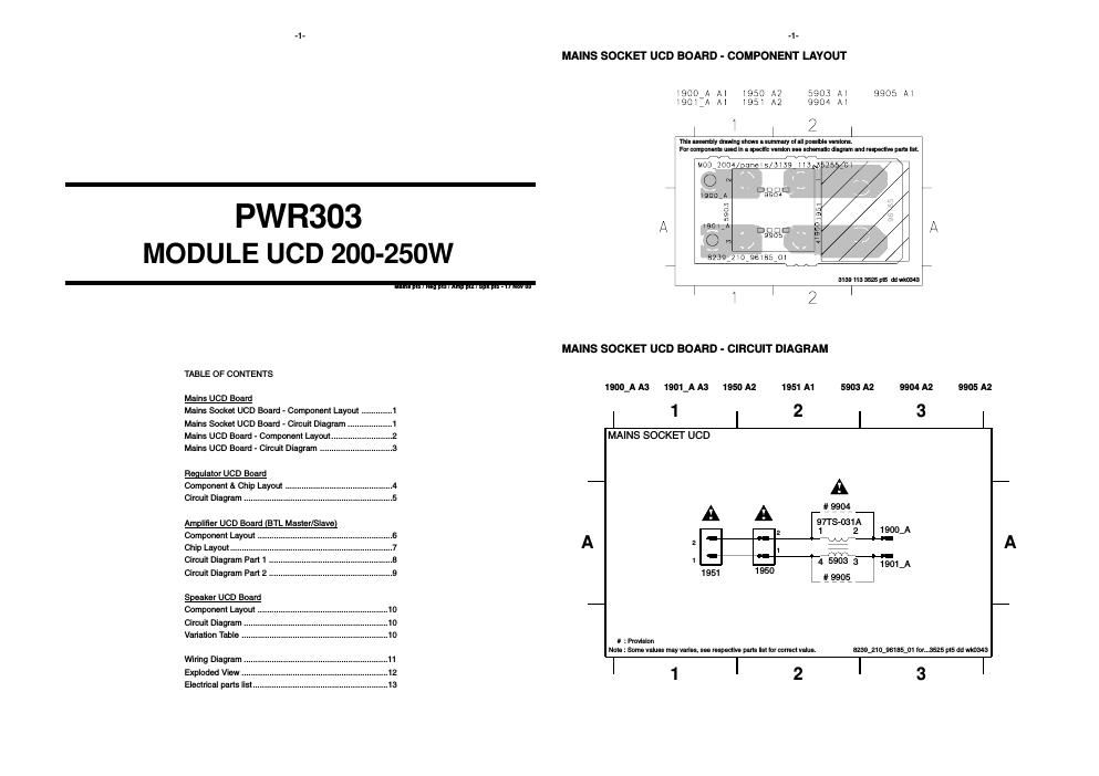
PWR303
MODULE UCD 200-250W

Mains pt5 / Reg pt3/Amp pm

TABLE OF CONTENTS

Mains UCD Board

Mains Socket UCD Board - Component Layout ............. 1
Mains Socket UCD Board - Circuit Diagram ..
Mains UCD Board - Component Layout ..... .
Mains UCD Board - Circuit Diagram ............................... 3

Regulator UCD Board
Component & Chip Layout ..

Circuit Diagram

Amplifier UCD Board BTL Master/Slavel
Component Layout .......................................................... 6

Chip Layout ...................................................................... 7
Circuit Diagram Part1
Circuit Diagram Part 2

Speaker UCD Board
Component Layout ........................................................ 10

Circuit Diagram
Variation Table .

Wiring Diagram
Exploded View .
Electrical parts list .......................................................... 13

pk pl5 - 17 Nov 03

.1.

MAINS SOCKET UCD BOARD - COMPONENT LAYOUT

l l950 A2 5903 Al
l 195l A2 9904 Al

This assembly drawing shows a summary oi all possible versions.
For components used in a specific version see schematic diagram and respective parts list.

9905 Al

MOD72OO4/poflels/3l39 113

O N

255701

l

i l:ll:|l:|l:| i
lSOOiA 9904

N, a

o m

a m

m a

O

A AQOAA l:ll:ll:ll:l 9 A

O 9905 2

V]

l

82397210796185701

3139 113 3525 p15 dd kaSAS

MAINS SOCKET UCD BOARD - CIRCUIT DIAGRAM

1900_A A3 1901_A A3 1950 A2 1951 A1 5903 A2

1 2 3

9904 A2

9905 A2

MAINS SOCKET UCD

_ A
A A 7419904 7

97TS-031 A
2 1 2 19007A
A 2 7
1 7
1 4 5903 3 19017A
1951 1950 # 9905

# :Provision
Note : Some values may varies, see respective parts list tor correct value.

8239,210>96185_01 for...3525 p15 dd wk0343

1 2 3

Page 2

-2- .2.

MAINS UCD BOARD - COMPONENT LAYOUT

0706 A5 190048 B9 2702 02 2712 B4 2909 E5 3705 c2 3902 D3 5904 c4 6707 61 6717 02 6905 D3 7901 D3 9934 A3 9945 07 9955 E7
1700 A3 190178 89 2703 01 2713 A2 2913 03 3706 02 3903 03 5929 04 6708 02 6718 A5 6906 D4 7902 E3 9935 A3 9946 07 9956 E7
1701 A1 1902 09 2704 B7 2714 A2 2916 D3 3707 A2 3904 E2 5930 E3 6709 B1 6719 A5 6912 E2 7903 D3 9936 B5 9947 08 9957 E7
1706 A5 1903 09 2705 A7 2715 A3 2917 03 3708 A2 3906 02 5931 E4 6710 B2 6720 A4 6913 E3 9901 05 9937 A7 9946 C8 9956 E8
1707 B7 1904 c9 2706 A6 2900 E4 2918 c3 3709 A2 3909 D3 6701 B2 6711 62 6721 B4 6916 c3 9902 D4 9938 A7 9949 C8 9959 A1
1708 B7 1905 C4 2707 A7 2902 E4 3700 B3 3710 A1 3912 05 6702 B2 6712 A7 6722 A5 6917 92 9903 A5 9940 C6 9950 D8
1710 89 1907 E9 2708 A6 2905 E2 3701 B3 3711 A2 3915 D3 6703 B2 6713 A5 6723 A4 7700 B1 9930 A1 9941 C6 9951 D8
1711 B8 1909 D4 2709 A5 2906 E3 3702 A2 3712 81 3916 E3 6704 B2 6714 B2 6900 E3 7701 A2 9931 A1 9942 C6 9952 E9
1712 BB 2700 02 2710 A4 2907 02 3703 A1 3900 05 3917 04 6705 A1 6715 A2 6901 02 7702 A2 9932 A1 9943 07 9953 E6
1713 88 2701 02 2711 A4 2908 E5 3704 B1 3901 D2 5900 D5 6706 A1 6716 A2 6902 D2 7900 02 9933 B1 9944 07 9954 E7
1 1 1 2 1 3 1 4 1 5 1 5 1 7 1 8 1 9
This assembly drawing shows a summary of all possible versions. For components used in a specific version see schematic diagram and respective parts list.
# / OD72OO4/pomelS/31397l13735255701 E:>
O . OD_2'@O¢Y15@>%:Q:1§L§§$©_210_9617 -
E
i
C ' ES]
[7
E >
S
N V
9
K 2
3139 113 3525 pt5 dd wk0343

l 1 2 3 4 5 6 7 8 ' 9