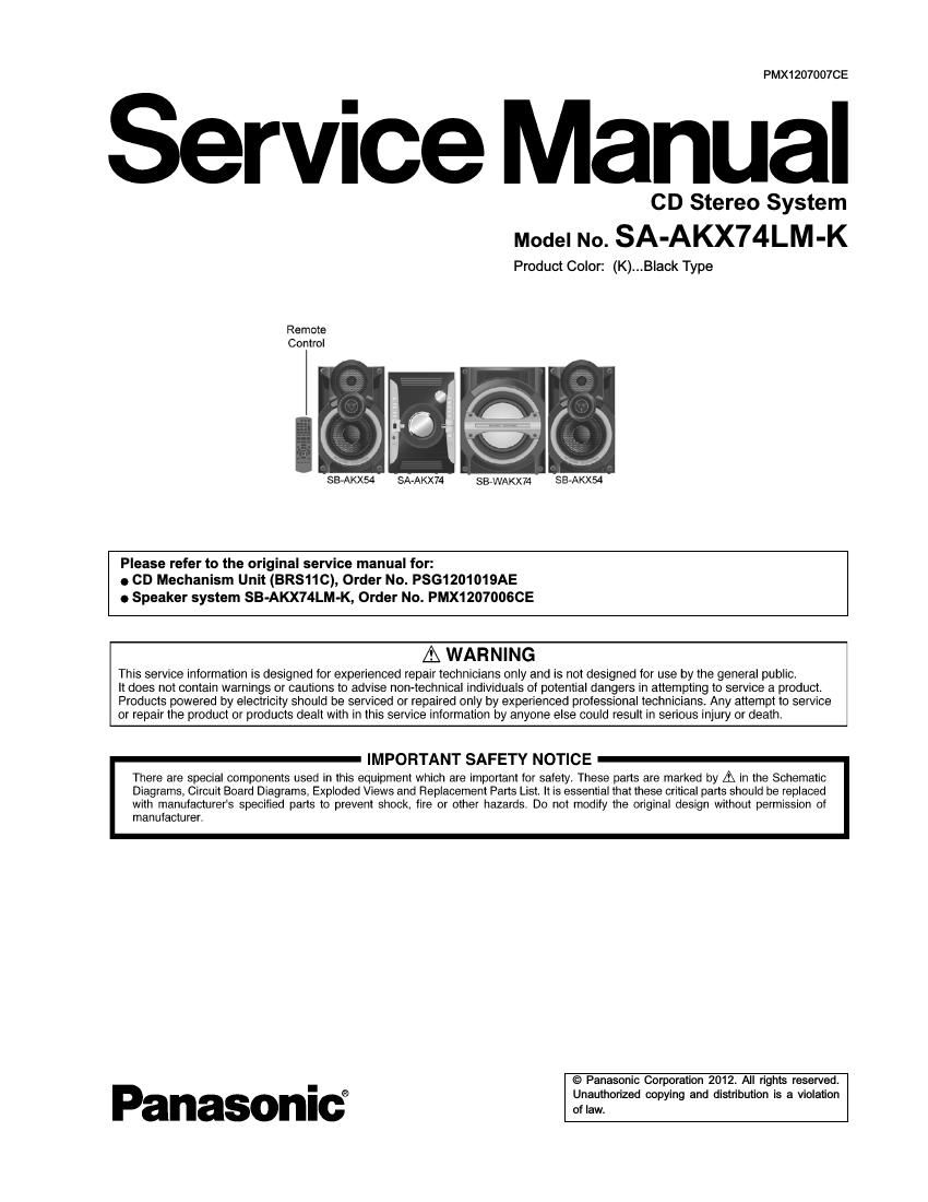
Panasonic sa akx74lm k

This is the 139 pages manual for panasonic sa akx74lm k.
Read or download the pdf for free. If you want to contribute, please mail your pdfs to info@audioservicemanuals.com.

Page: 1 / 139
left right
panasonic sa akx74lm k

Extracted text from panasonic sa akx74lm k (Ocr-read)


Page 1

TABLE OF CONTENTS 1 Safety Precautions 1.1. General Guidelines 1.3. Before Repair and Adjustment 1.4. Protection Circuitry 1.5. Caution For Fuse Replacement 1.6. Safety Parts Information 2 Warning 2.1. Prevention of Electrostatic Discharge (ESD) to Electrostatic Sensitive (ES) Devices 2.2. Precaution of Laser Diode 2.3. Service caution based on Legal restrictions 2.4. Handling Precautions for Traverse Unit 3 Service Navigation 3.1. Service Information4 Specifications 5 General/Introduction 5.1. Media Information 6 Location of Controls and Components 6.1. Remote Control Key Button Operation 6.2. Main Unit Key Button Operation 7 Installation Instructions 7.1. Speaker and A/C Connection 8 Service Mode 8.1. Cold-Start 8.2. Doctor Mode Table 8.3. Reliability Test Mode (CD Mechanism Unit (BRS11C)) 8.4. Self-Diagnostic Mode 8.5. Self-Diagnostic Error Code Table Please refer to the original service manual for: CD Mechanism Unit (BRS11C), Order No. PSG1201019AE Speaker system SB-AKX74LM-K, Order No. PMX1207006CE Nota: El idioma original de este Manual de Servicio es en idioma inglés, sin embargo algunas notas aquí mencionadas serán escritas en español para mejor descripción para Centros de Servicio de México. 2

Page 2

8.6. Sales Demonstration Lock Function 9 Troubleshooting Guide 9.1. Part Location 9.2. Troubleshooting Guide for F61 and/or F76 9.3. D-Amp IC Operation & Control 10 Service Fixture & Tools 11 Disassembly and Assembly Instructions 11.1. Disassembly Flow Chart 11.2. Main Components and P.C.B. Locations 11.3. Disassembly of Top Cabinet 11.4. Disassembly of Front Panel Unit 11.5. Disassembly of Mic P.C.B. 11.6. Disassembly of Panel P.C.B. 11.7. Disassembly of Memory LED P.C.B. 11.8. Disassembly of Remote Sensor P.C.B. 11.9. Disassembly of USB P.C.B. 11.10. Disassembly of Music Port P.C.B. 11.11. Disassembly of Top Bar LED P.C.B. 11.12. Disassembly of Bottom Bar LED P.C.B. 11.13. Disassembly of Main P.C.B. 11.14. Replacement of Voltage Regulator IC (IC2010) 11.15. Replacement of Voltage Regulator IC (IC2011) 11.16. Replacement of Audio Digital Amp IC (IC5800) 11.17. Replacement of Audio Digital Amp IC (IC5700) 11.18. Disassembly of D-Amp P.C.B. 11.19. Replacement of Audio Digital Amp IC (IC5900) 11.20. Disassembly of SMPS P.C.B. 11.21. Replacement ofSwitching Regulator IC (IC5701) 11.22. Replacement of Rectifier Diode (D5702) 11.23. Replacement of Rectifier Diode (D5801) 11.24. Replacement of Rectifier Diode (D5802) 11.25. Replacement of Regulator Diode (D5803) 11.26. Disassembly of CD Mechanism Unit (BRS11C) 11.27. Disassembly of CD Interface P.C.B. 11.28. Disassembly of CD Servo P.C.B. 11.29. Disassembly of Rear Panel 12 Service Position 12.1. Checking and Repairing of Main P.C.B. 12.2. Checking and Repairing of D-Amp P.C.B. 12.3. Checking and Repa iring of Panel P.C.B. 12.4. Checking and Repairing of SMPS P.C.B. - 12.5. Checking and Repairing of CD Servo P.C.B. (Side A) 12.6. Checking and Repairing of CD Servo P.C.B. (Side B) 13 Simplified Block Diagram 13.1. Power Block Diagram 14 Block Diagram 14.1. Servo & System Control 14.2. IC Terminal Chart 14.3. Audio 14.4. Power Supply 15 Wiring Connection Diagram16 Schematic Diagram 16.1. Schematic Diagram Notes 16.2. CD Servo Circuit 16.3. Main(MICON) Circuit 16.4. Main(D-Amp) Circuit 16.5. Panel Circuit 16.6. Remote Sensor, USB, Music Port , Memory LED, Top Bar LED and Bottom Bar LED Circuit 16.7. CD Interface, Mic and Voltage Selector Circuit 16.8. D-Amp Circuit 16.9. SMPS Circuit 17 Printed Circuit Board 17.1. CD Servo P.C.B. 17.2. Main P.C.B. (Side A) 17.3. Main P.C.B. (Side B) 17.4. Panel, Remote Sensor , USB and Music Port P.C.B. 17.5. Memory LED, CD Interface, Top Bar LED, Bottom Bar LED and Mic P.C.B. 17.7. SMPS and D-Amp P.C.B. 18 Appendix Information of Schematic Diagram 18.1. Voltage & Waveform Chart 18.2. Illustration of ICs, Transistor and Diode 18.3. Terminal Function of ICs 19 Exploded View and Replacement Parts List 19.1. Exploded View and Mechanical replacement Part List 19.2. Electrical Replacement Part List 3