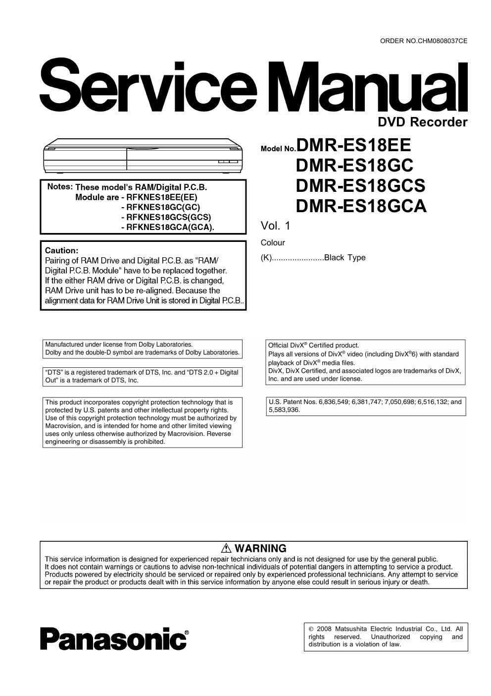
Panasonic dmr es 18 ee service manual

This is the 85 pages manual for panasonic dmr es 18 ee service manual.
Read or download the pdf for free. If you want to contribute, please mail your pdfs to info@audioservicemanuals.com.

Page: 1 / 85
left right
panasonic dmr es 18 ee service manual

Extracted text from panasonic dmr es 18 ee service manual (Ocr-read)


Page 1

ORDER NO.CHM0808037CE

Service Manual

Notes: These model's RAM/Digital P.C.B.
Module are - RFKNES18EE(EE)
- RFKNES18GC(GC)
- RFKNES1BGCS(GCS)
- RFKNES18GCA(GCA).

Caution:

Pairing of RAM Drive and Digital P.C.B. as "RAM/
Digital PCB. Module" have to be replaced together,

If the either RAM drive or Digital P.C.B. is changed,
RAM Dr'we unit has to be re-aligned. Because the
alignment data for RAM Drive Unit is stored in Digital P.C.B..

DVD Recorder

ModemoDMR-ES18EE
DMR-ES1SGC
DMR-ES1BGCS
DMR-ES1BGCA

Vol. 1

Colour

(K) ....................... Black Type

Manufactured under license from Dolby Laboratories.
Dolby and the double-D symbol are trademarks of Dolby Laboratories.

DTS is a registered trademark of DTS, Inc. and DTS 2.0 + Digital
Out is a trademark of DTs, Inc.

Oflicial DivX® Certified product.

Plays all versions of DivX® video (including DivX®6) with standard
playback ot DivX) media files.

DivX, DivX Certified, and associated logos are trademarks of DivX,
Inc. and are used under license.

This product incorporates copyright protection technology that is
protected by U.S. patents and other intellectual property rights.
Use of this copyright protection technology must be authorized by
Macrovision, and is intended lor home and other limited viewing
uses only unless otherwise authorized by Macrovision. Reverse
engineering or disassembly is prohibited.

US. Patent Nos. 6,836,549; 6,381 ,747; 7,050,698; 6,516,132; and
5,583,936.

AWARNING

This service information is designed for experienced repair technicians only and is not designed for use by the general public.

It does not contain warnings or cautions to advise non-technical individuals of potential dangers in attempting to service a product.
Products powered by electricity should be serviced or repaired only by experienced professional technicians. Any attempt to service
or repair the product or products dealt with in this service information by anyone else could result in serious injury or death.

Panasonic?

© 2008 Matsushita Electric Industrial Co., Ltd. All
rights reserved. Unauthorized copying and
distribution is a violation of law.

Page 2

DMR-E51EEE I DMRAE51BGC I DMR-ES1BGCS I DMR-ES1BGCA

CONTENTS

1 Safety Precaution -----
1.1. General guidelines

2 Warning ----------------------
2.1. Prevention of Electrostatic Discharge (ESD) to
Electrostatic Sensitive (ES) Devices ................................ 4
2.2. Precaution of Laser Diode .............................................. 5
2.3. SerVICe caution based on legal restrictions ...................... 5
3 Service Navigation .................................................................. 7
3.1. Service Information -------------------------------------------------------- 7

3.2. Caution for DivX-

4 Specifications-


5 Location of Controls and Components

6 Operation Instructions ..................... .12
6.1. Taking out the Disc from DVD-Drive Unit when the Disc

cannot be ejected by OPEN/CLOSE button ................... 12

7 Service Mode --------------------------------------------------------------------- 16

7.1. SelfDiagnosis and Special Mode Setting ...................... 15

8 Service Fixture 8. Tools ........................................................ 24

9 Disassembly and Assembly Instructions .............................. 25

9.1. Disassembly Flow Chart-
9.2. P.C.B. Positions-

9.3. Top Case -----

9.4. Front Panel ------------------------------------------------------------------ 27
9.5. Front (L) P.C.B., Front (R) P.C.B. --------------------------------- 28
9.6. RAM/Digital P.C.B. Module ---------------------------------- 28
9.7. DV P.C.B. -------------------------------------------------------------------- 29
9.8. Rear Panel, Fan Motor ------------------------------------------------- 30
9.9. Power P.C.B. --------------------------------------------------------------- 30

9.10. Main P.C.B., SW P.C.B.----

10 Measurements and Adjustments

10.1. Service Positions
10.2. Caution for Replacing Parts
10.3. Standard Inspection Specifications after Making Repairs-36

11 Block Diagram ---------------------------------------------------------------------- 37
11.1. Power Supply Block Diagram ........................................ 37
11.2. Analog Video Block Diagram ........................................ 39
11.3. Analog Audio Block Diagram ---------------------------------------- 40
11.4. Analog Timer Block Diagram ........................................ 41

12 Schematic Diagram -----------

12.1. Interconnection Schematic Diagram

12.2. Power Supply Schematic Diagram

Page

12.3. Main Net (1/4) Section (Main P.C.B. (1/4)) Schematic
Diagram (M)
12.4. Main Net (2/4) Section (Main P.C.B. (1/4)) Schematic

--45

Diagram (M) ----------------------------------------------------------------- 46
12.5. Main Net (3/4) Section (Main P.C.B. (1/4)) Schematic
Diagram (M) ----------------------------------------------------------------- 47
12.6. Main Net (4/4) Section (Main P.C.B. (1/4)) Schematic
Diagram (M) ----------------------------------------------------------------- 48
127. AV l/O (1/4) Section (Main P.C.B. (2/4)) Schematic
Diagram (AV) -------------------------------------------------------- 50
12.8. AV l/O (2/4) Section (Main P.C.B. (2/4)) Schematic
Diagram (AV)- --51
12.9. AV l/O (3/4) Section (Main P.C.B. (2/4)) Schematic
Diagram (AV) --------------------------------------------------------------- 52
12.10. AV [/0 (4/4) Section (Main P.C.B. (2/4)) Schematic
Diagram (AV) ----------------------------------------------------- 53
12.11. Tuner Section (Main P.C.B. (3/4)) Schematic Diagram
(TU) ------------------------------------------------------- 55
12.12. Timer (1/4) Section (Main P.C.B. (4/4)) Schematic
Diagram (T)--- -------------------------------------------- 57
12.13. Timer (2/4) Section (Main P.C.B. (4/4)) Schematic
Diagram (T) --------------------------------------------------- 58
12.14. Timer (3/4) Section (Main P.C.B. (4/4)) Schematic
Diagram (T) --------------------------------------------------- 59
12.15. Timer (4/4) Section (Main P.C.B. (4/4)) Schematic
Diagram (T)--- ---------------------------------------------------- 60
12.16. DV Schematic Diagram ------------------------------------------------ 61
12.17. SW Schematic Diagram ----------------------------------------------- 61

12.18. Front (L) Schematic Diagram

12.19. Front (R) Schematic Diagram

13 Printed Circuit Board-

13.1. Power P.C.B.--
13.2. Main P.C.B.-

13.3. Front (L) P.C.B., Front (R) P.C.B., Sw P.C.B. and DV


P.C.B. ----------------------------------------- 69
14 Appendix for Schematic Diagram ----------------------------------------- 71

14.1. Voltage and Waveform Chart --------------------------------------- 71
15 Parts and Exploded Views ---------------------------------------------------- 77

15.1. Exploded Views
15.2. Replacement Parts Lis