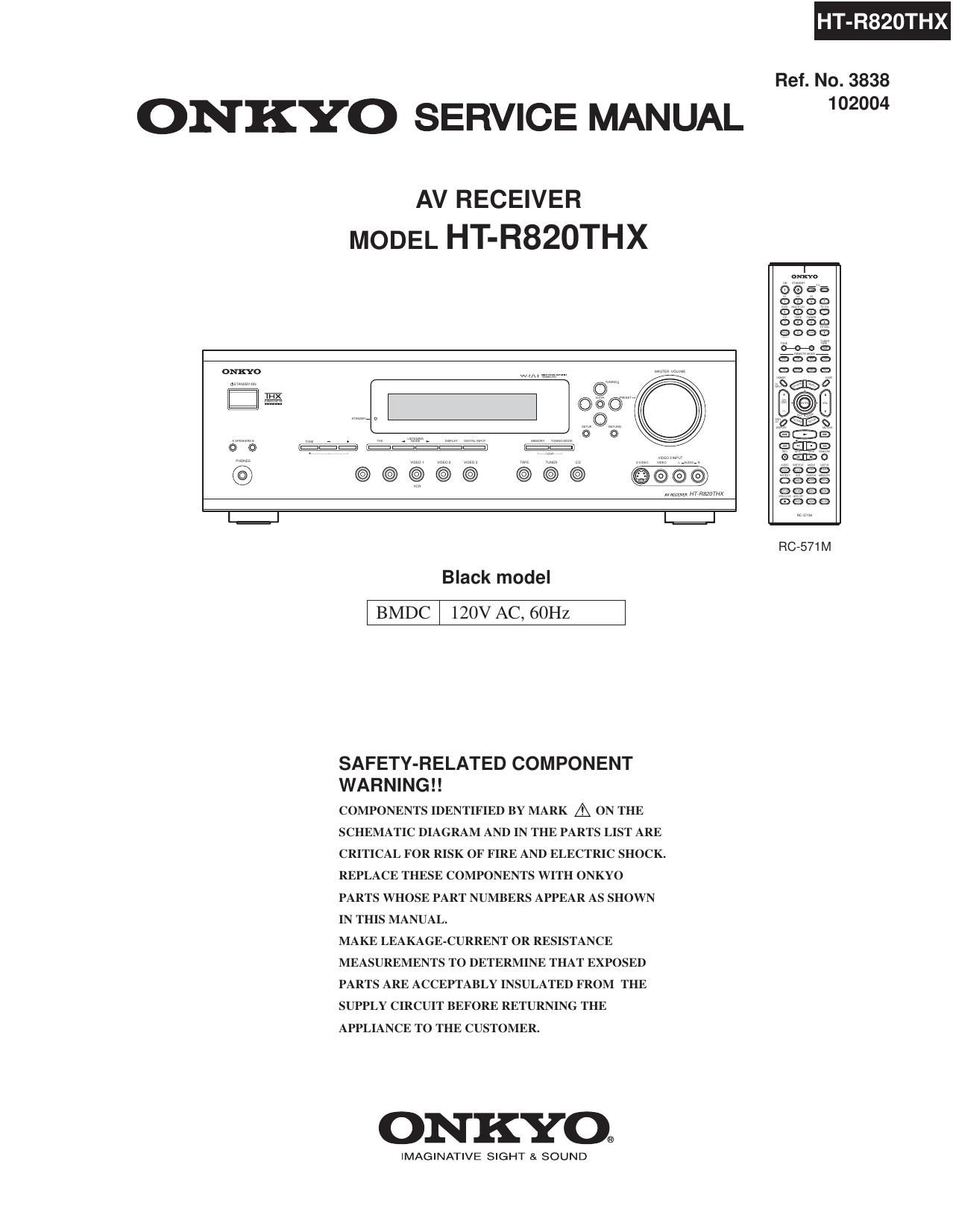
Onkyo HTR 820 THX Service Manual
This is the 141 pages manual for Onkyo HTR 820 THX Service Manual.
Read or download the pdf for free. If you want to contribute, please upload pdfs to audioservicemanuals.wetransfer.com.
Page: 1 / 141