Moog mf 105m murf notice

This is the 14 pages manual for moog mf 105m murf notice.
Read or download the pdf for free. If you want to contribute, please mail your pdfs to info@audioservicemanuals.com.

Page: 1 / 14
left right
moog mf 105m murf notice

Extracted text from moog mf 105m murf notice (Ocr-read)


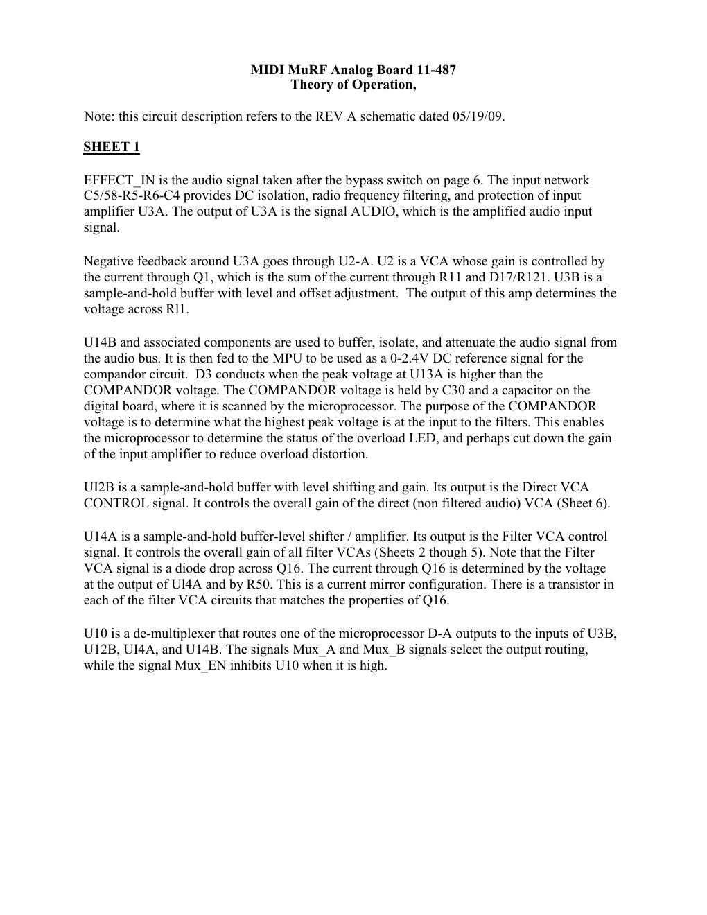
Page 1

SHEET 2 U5B is a comparator and level shifter that takes the signal from the MPU and converts it from 0-3.3V to +/ -5V with some hysteresis. This signal is used by the Mux switches to select the regular or base voicing of the filters. U5A works in the same way as U5 to convert a duty cyc le modulated PWM signal from the MPU to be used as the shift input to the SHIFT Mux. The duty cycle of this PWM affects the actual frequency center of the filters. R145/R131/R176 are used to limit the +/ -5V swing slightly to avoid some distortion artifacts in the CD4016. SHEETS 2 - 5 Sheets 2 through 5 s how all eight filters with their respective filter VCAs. With the exception of the first filter, the circuits are identical topology. Only the two capacitors and two resistors that set the frequency for eac h bank change for voice. We will first describe Filters 2 through 8 as they are all the same and then discuss the difference with filter 1. Each filter has two modes of primary operation. Those are called Mid Frequency mode and Base Frequency mode. Norma l operation is in Base mode. Mid Frequency Mode is accomplished by three 4016 switches that switch three parallel resistors around the circuit to slightly skew the resonant frequency by slightly less than one octave. First describing base frequency mode: Filter twos AUDIO signal is applied to the filter through R55. The filter is a first order band pass filter which consists of U13B, C33, C32, R54 and R66. The output of the filter is at U13B -7. U23C and U23B switch on and off in response to the SHIFT waveform. When these switches are on, the filter resonant frequency is raised by about 30%, because R65 and R67 are placed in parallel with R66 and R54 respectively. When the switches are off, the filter resonant frequency is not raised. As the duty cycle of the SHIFT signal increases from about 20% to 80%, the resonant frequency increases about 10%. To switch from the base voicing to mid frequency voicing the MID_voicing logic signal from U5B is applied to 2 4016 gates. These gates close two parallel resistors, in this case R146 and R168 around the filter resistors to change the frequency about an octave. All filters act as described above with the exception of filter 1. Filter 1, when switched to base voicing, bypasses the band pass filter and swaps it out with a 2 nd order low pass filter. U15C and U15B swap these out. Filter 1 uses a DG445 rather than a CD4016 so that it can run from the 9V rails and, hence give more headroom and less distortion. D116/R136 is used to convert the selector signal to +5/ GND fom +/ -5V for U15 and R152/Q51/R150 invert this signal for the base voicing.

Page 2

The output of the filter is applied through C28 and R41 to the bases of Q10 and Q6. The transconductance of this transistor pair is proportional to the current through them, which is the same as the current through Q9. The network of U11B, R40, and Q5 is a voltage -to -current converter. The input VCA_2 from the digital board is the envelope voltage for Filter 2. It goes from 0V to +2.4 volts. The voltage at U11B -7 is such that the current through Q5 in milliamperes is numerically equally to the voltage at the input to the op amp. Note that U11 has voltage rails of +9 but only - 5. This is to limit the off condition of the output to not swing below - 5V and reverse bias Q11. The current through Q9 is a fraction of the current through Q5. This fraction is determined by the voltage across R34. If the voltage across R34 is zero, then the current through Q9 is equal to the voltage across Q5. This is very nearly the case when Q12 is s hut off. However, when Q12 conducts, there is a voltage drop across R34, and the current through Q9 is reduced to a fraction of the current through Q5. This fraction depends only on FILT_VCA_CV, which, in turn, depends on the voltage at the output of Ul4A (Sheet 1). This is how a single voltage at the output of Ul4A determines the overall gains of all filter VCAs, regardless of the status of the envelopes. The collectors of Q10 and Q6 form a balanced differential pair that is bussed to the corresponding outputs of the other even filter numbers. This buss then goes to the summing inputs of the "EVEN or RIGHT output amplifier (Sheet 6). Similarly, the collector outputs of the off filters (FILT 1, FILT 3, FILT 5, and FILT 7) are bussed and go to the summing inputs of the "ODD" or LEFT amplifier. SHEET 6 The DIRECT VCA is shown in the upper left corner of the sheet. It is actually two VCAs. One VCA is for the "RIGHT" side summing amplifier, while the other VCA is for the "LEFT" side summing amplifier. Th us, the direct signal is fed equally to both audio outputs. The amount that is fed is determined by the DIRECT_VCA -CV signal (U12B sheet 1), which is derived from the settings of the MIX and the OUTPUT panel controls on the digital board. Note that the D irect VCA is fed out of phase to the summing amps from the filter VCAs. This is to compensate for the phase inversion of the filter amplifiers when adding direct signal back in. U8A and U8B are the two output amplifiers. They are classic 4 resistor balanc ed differential amplifiers with the two input resistors being the impedance of the transistor pairs. Q2 supplies a smoothed bias voltage of about +7 volts that enables the collectors of the filter VCA's to be connected directly to the inputs of U8A and U8B . U6 performs the bypass/on switching functions. The switch signal BYPASS comes from the digital board. This bypass switch diverts the AUDIO_IN from the jack board either to the Page 1 input filter or directly out as well as switching the output signal fr om the U8 op amps to the input signal. The audio feeds to the LEFT/MONO OUT and RIGHT OUT jacks on the jack board. They are summed to mono on the jack board. Note that when the MFI05 is in bypass, the bypass output appears only at the LEFT/MONO jack unle ss JMP11 solder blob is shorted.