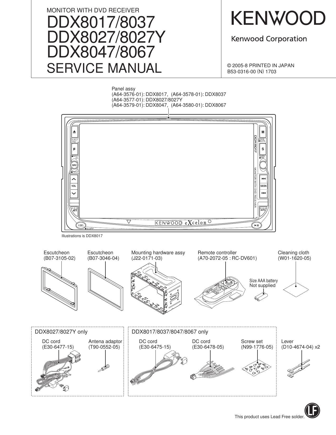
Kenwood DDX 8017 Service Manual

This is the 114 pages manual for Kenwood DDX 8017 Service Manual.
Read or download the pdf for free. If you want to contribute, please mail your pdfs to info@audioservicemanuals.com.

Page: 1 / 114
left right
Kenwood DDX 8017 Service Manual

Extracted text from Kenwood DDX 8017 Service Manual (Ocr-read)


Page 2

DDX8017/8027/8027Y
DDX8037/8047/8067

NOTES ON ASSEMBLING THE MECHANISM

1. Fasten Screw A so that the interval (a) will be about 5.2mm
and the interval (b) will be about 2.6mm (The interval (a)
can be measured using a pair of vernier calipers or similar
tools.)

2. Turn B so that Position (0) will come at about the center of
interval (d).

3. Then, play the test disc and fine tune A or B so that the jitter
value would be minimized.

Page 13

DDX8017/8027/8027Y

DDX8037/8047/8067

COMPONENTS DESCRIPTION

Ref. No. Application/ Function Operation] Condition] Compatibility
0209 For audio muting Audio muting of AVOUT left channel
0250 AM power supply SW Comes ON when AM source is selected
0252 For AM power supply Audio 8V is supplied when AM source is selected
0403,404 SW for audio selector control Converts IC413 p-com controlled terminal voltage: 5V ~> 8V
0405,406 SW for audio selector control Converts IC414 p-com controlled terminal voltage: 5V ~> 8V
0500 For reversing resetting signal voltage Reverses signal in order to obtain resetting signal for TV tuner
0800 MUTE 0 terminal control SW MUTE 0 audio muting control
0 VIDEO UNIT (X35-458/459X-10)
Ref. No. Application/ Function Operation] Condition] Compatibility
IC1 Inverter control IC Control and drive oi inverter circuit for backlight
IC101 DC/DC converter IC i12V power supply for VCOM amp, -12.0V/+18.5V LCD power supply
l0203 VCOM amp VCOM srgnal amplification amp
IC300 Three states buffer Start pulse switching SW
IC301 Timing controller lC LCD module control
|0302 AND V.SYNC delay buffer
IC303 PLL LPF LPF for PLL control (VT voltage control)
l0601 Remote controller light receptor IC Remote controller light receptor
01 Dimmer SW ON/OFF control signal oi PWM and put on dimmer on backlight
02,3 Inverter driver Inverter circuit driving
05 5V AVR 5V power supply for inverter control IC
0101 Switch Switch for controlling DC/DC converter
0102 Switch Switch lor controlling DC/DC converter
0202,203 VCOM driver VCOM signal bufler
0300 Switch For switching IC205
0301 VCO For PLL oscillation
0302 Touch panel X1 SW X1 SW: Comes on at panel touch detection or at X-axis input and impresses voltage
0303 Touch panel Y1 SW Y1 SW: Comes on at Y-axis input and impresses voltage
0304 Touch panel X0 SW X0 SW: Comes on at X-axis input and impresses voltage
0305 Touch panel Y0 SW Y0 SW: Comes on at Y-axis input and impresses voltage
0306 Touch panel Y0/Y1 SW Y0/Y1 SW: Comes on at Y-axis input and goes off at X-axis input
0307,308 Buffer For PLL clock
0601 ,602 Switch SI blinking switch
0604,605 Switch Hard resetting switch
0701 Switch DISC Illumination switch
0 DAUGHTER UNIT (X89-274/279x-11)
Ref. No. Application/ Function Operation] Condition] Compatibility
IC2 OP amp For audio signal amplification (Center, Sub-woofer)
|C3 OP amp For audio signal amplification (Rear)

13

Page 22

DDX8017/8027/8027Y
DDX8037/8047/8067

MICROCOMPUTERS TERMINAL DESCRIPTION

Pin No. Pin Name Module l/O Application Processing Operation Description
164 MD2 EXTRA | Clock mode setting Low level fixed
165 SHiRST V850 |
166 CA EXTRA | Hardware standby request High level fixed
167 MD3 EXTRA | 030 space bus width designation Low level fixed
168 MD4 EXTRA | 080 space bus width designation High level fixed
169 MD5 EXTRA | Endean setting Low level fixed
170 Avss Power supply -

171 XDATA X35 | Touch panel input (X-direction)

172 YDATA X35 | Touch panel input (Y-direction)

173,174 NC 0

175 Avcc Power supply - Power supply for analog 3.3V
176 AVss Power supply -

0 Audio Microcomputer: 703068YGJ128A (X34: ICSOS)

Module Truth Value
Pin No. Pin Name l/O Application Processing Operation Description
(physical) Table
1 DCiERR ICZ VI | DC offset detection Low at the detection
Normal: 1.6V, TEL MUTE: 1V or lower,
2 LINEiMUTE DC-CN | LINE MUTE detection
NAVI MUTE: 2.5V or higher
3,4 NC NC
5 PORTGNDO uCOM

LX/NAVll/SWS (orTV)/ 7
6 AUD|078W17A Audio 0 (1) Refer to truth value table
AV|N1 audio switching (For main)

LX/NAVI1/SW3 (orTV)/

7 AUDI078W1iB Audio 0 (1) Refer to truth value table
AV|N1 audio switching (For main)
8 AUDI078W27A Audio 0 TV/AVIN1/AVIN2 audio switching (For sub) (2) Refer to truth value table
9 AUD|078W27B Audio 0 TV/AVIN1/AVIN2 audio switching (For sub) Q) Refer to truth value table
10,11 NC 0
12~14 NC NC 0
15 NC 0 L: MUTE ON, H: MUTE OFF
16 NC 0
17 NC NC 0
When writing to E2PROM from outside,
Hi is input with a)ig. (Common use SCL
18 EEPROM7WRT EEPROM | Write detection at ROM correction
and SDA will stop operation)
In other cases: Low (Pull-down)
19 MUTEiAVOUT MUTE O MUTE for AVOUT L: MUTE ON, H: Normal
20 MUTEiPRE MUTE O MUTE for PREOUT L: MUTE ON, H: Normal

22

Page 25

DDX8017/8027/8027Y
DDX8037/8047/8067

MICROCOMPUTERS TERMINAL DESCRIPTION

Module TruthValue
Pin No. Pin Name No Application Processing Operation Description
(physical) Table
94 DACiDO DSP BLOCK | Communication data for DAC
94 DSPisO DSP BLOCK | Communication data for DSP
95 DACiDI DSP BLOCK 0 Communication data for DAC
95 DSPisI DSP BLOCK 0 Communication data for DSP
96 FSEL71 DSP BLOCK 0 Frequency selection for DC/DC
97 FSEL72 DSP BLOCK 0 Frequency selection for DC/DC
98 NC NC 0
NTSC/PAL identification COMP signal
99 VSYN078W2 Visual 0 Switching tor monitoring whether there is @
AUTO detection COMP signal or not
100 TYPE4 TYPE I 0) Refer to truth value table
101 TV700N TV 0 Start up request to TV unit H: TV unit ON, L: TV unit OFF
102 PORTVDD2 uCOM
103 TViCLK TV 0 Clock to TV unit
104 TViMREQ TV 0 Request to TV unit
105 TViMDATA TV 0 Data to TV unit
106 TVisDATA TV | Data lrom TV unit
107 LX7DATA7S LX7M | Data lrom slave unit
108 LX7DATA7M LX7M 0 Data to slave unit
109 inCLK LX7M I/O LX BUS clock
110 VISUALSWSJ Visual O TV/AVIN1 video switching (13 Refer to truth value table
111 NAV|17RX NAVI | Data from navigation 1
112 NAV|17TX NAVI 0 Data to navigation 1
113 VISUAL78W4 Visual O TV/Flear view camera video switching {2! Refer to truth value table
114 RGBisw Visual O TV/NAVI1/NAVI2 RGB video switching 60 Refer to truth value table
115 TViJUDGE TV | TV tuner old/new identification H: Old, L: New
NTSC/PAL identification COMP signal
116 VSYN078W1 Visual 0 Switching for monitoring whether there is (139
AUTO detection COMP signal or not
1 17,1 18 NC
119 VISUAL73W372 Visual O NAVI1/NAVI2/AVIN2 video switching ® Refer to truth value table
Vertical synchronization signal detection
120 VSYNCiDET Visual |
(For AV|N2 automatic detection)
121 VISUALSWBJ Visual O NAVI1/NAVI2/AVIN1 video switching ® Refer to truth value table
122 VISUAL75W272 Visual O SW5 (or TV)/AV|N2/DVD video switching (9) Refer to truth value table
123 VISUAL,SW271 Visual O SW5 (or TV)/AV|N2/DVD video switching (9) Refer to truth value table
AVIN2/SW5 (or TV)/
124 VISUAL75W172 Visual O (8) Refer to truth value table
SW3 (or NAVI1) video switching
125 RDSicLK RDS | RDS decoder CLK input

25

Page 31

DDX8017/8027/8027Y
DDX8037/8047/8067

TEST MODE

0 Information Screen

Below are display contents of the Information Screen.

- Region Code

- Serial No.

- Graphic uCom Version

- System uCom Version / Rom Correction Version (Type

- F/E Version / B/E Version

- Macrovision Version

- Box uCom Version / Rom Correction Version /Type / Span
(Tuner frequency Span information)

- DC Offset detection information

' Security Info (BLANK: E2PROM not written, ON/OFF: Nor-
mal condition (ON/OFF security is set), ERROR: E2PROM
write abnormal)

O TOUCH Screen

- Adjust Touch position and write it on E2PROM.

- With 3-point input, write from system p-com to EEPFIOM is
achieved.

- E2PROM normal/abnormal ending is displayed on screen.

0 HPOSI Screen

- Screen position adjustment is conducted and the result is
stored in E2PROM.
Adjustments are conducted in the following order:
DVD -> TV -> VIDEO -> NAVI

- DVD wallpaper is NTSC-fixed.

. E2PROM write normal/abnormal ending is displayed on
screen.

' While adjustment is conducted on DVD, TDV-540A (Title 3»
Chapter 16) is played.
After Disc Loading, by pressing Tenkey [4] on the remote
controller, transition is made to Title 3-Chapter16.

O SERVICE Screen

Shown below are contents of the Service Screen.

- Power On time

. DVD Play time / DVD Eject number of times

- Monitor Open number of times / Monitor Close number of
times

- E2PROM Chroma data information

- DC Offset detection information

Writing Serial No.
By pressing the Serial key, transition to the Serial No. Input
screen is made.

E2PROM Chroma Data Clear
By pressing the Clear key, the E2PROM Chroma data is
cleared.

DC Offset Data Clear
By pressing the Clear key, the E2PROM DC Offset data is
cleared.

O Chroma Screen

- Chroma adjustment is conducted and the result is stored in
E2PROM.

- The setting procedures are conducted with a remote con-
troller.

- Chroma IC adjustment screen (Item setting) -> To be writ»
ten on EEPFIOM.
Setting item

VCO free run adjustment (00h~FFh)
YGCA gain adjustment (00h~FFh)
Brightness adjustment (00h~FFh)
Contrast adjustment (00h~FFh)

Black limiter adjustment (00h~7Fh)

White limiter peak adjustment (00h~7Fh)
Gamma 1 adjustment (00h~FFh)

Gamma 2 adjustment (00h~FFh)

Rch sub-brightness adjustment (00h~FFh)
Bch sub-brightness adjustment (00h~FFh)
Rch sub-contrast adjustment (00h~FFh)
Bch sub-contrast adjustment (OOh~FFh)
VCOM oscillation width adjustment (00h~FFh)

- E2PROM write normal/abnormal ending is displayed on
screen.

- Writing region does not clear EEPROM Chroma data.
EEPROM chroma data is cleared by the Clear key in the
Service screen.

0 MECHA ADJ Screen

- 2DIN panel adjustment is conducted and the result is stored
in E2PROM.

- The voltage values at the time of Full Open/Full Close are
written to E2PROM.

- E2PROM write normal/abnormal ending is displayed on
screen.

0 Source / Audio / Setup Screen
- Source/Audio Control/Setup Screen are the same as nor-
mal condition.

0 Display

- Basically, in the Test Mode, screen will be dedicated screen.

- There will be no opening screen.

- Even during seek, the frequency display will be made.

- Touch position display (+) will be made. However, no dis-
play will be made in the Touch Adjust screen (In adjust-
ment). 31

Page 42

DDX8017/8027/8027Y
DDX8037/8047/8067

42

ADJUSTMENT

2. Freerun Frequency Adjustment (X35: VR301)

Measurement Location
Adjustment
No. Adjustment Method Timing controller 1 DIN 2D|N Adjustment Value
Location
ICSOI X35-448 X35458
1 Set TP ot NVD TP as no input NVD (21pm) TP363B TP55
and connect to PON3.3V.
Set TP of NHD TP as no input and NHD (22pin) TP304B TP17
connect to PON3.3V.
2 Adjust frequency of HSYNC with NDSH (9pin) TP307B TP106 VR301 15.734kHZt0.01kHZ
a frequency counter. (NTSC type)
15.625kH2i0.01kHZ
(PAL type)

3. Flicker Adjustment (X35: VR203)
Condition (As usual)

Video source: VIDEO

Video: Luster white 30~50°/a

BRIGHT: MAX

MODE: ZOOM

Ad'ustment Procedure
1. Set to the above condition.

2. Vary VR203 and adjust so that the side width that appear
on screen top would become smallest.

4. Horizontal Display Start Position and
OSD Display Position Adjustment

7 Screen adjustment key: HPOSI i

Go tote next adjustment screen

Next
|:| Witt

|:|

OSD

|::| 94 X

i

l
Return to the menu screen

OSD adjustment key

|:|

Horizontal screen position adjustment

Screen Adjustment Key (HPOSI)

: Horizontal display start position adjustment of entire screen
OSD Adjustment Key

: Horizontal display start position adjustment of OSD only

About the video for ad'ustment screen
DVD: Monoscope (TDV-540A, Title :2. Chapter : 16)
TV: Monoscope
VIDEOt: Monoscope
Navigation: Input KNA-DV3200
* For NTSC area destination: NTSC video
For PAL area destination : PAL video
96 As for TV tuner Box, use the TV Tuner Box suited for each
destination.
* NAVI screen is NAVI Menu Screen.

Ad'ustment Procedure
1. Press HPOSI on Test Mode Menu Screen.

2. Adjust HPOSI display start position of the following five;
Graphic/DVD/TV/VIDEC/Navigation.

3-1. Graphic
Use OSD key to adjust so that background is not seen on
both sides of screen.
HPOSI key is not to be used. Pay attention not to used it. as
it can be operated on.

NG NG OK

Page 83

DDX8017/8027/8027Y
DDX8037/8047/8067

VIDEO LINE

SlGNAL LINE r N E F

GND LINE 3 § :1 E Z E E 8
<

*5 NE Z i Z 3 3 3 o 5

can R531
3 mu m

cm R532
we 3 a 7

cm R533
3 m

R53o 1K

Rana
K

R535 1K
5c coN

BF CLK
MC EEO
MC um
55 age

55 um

R535 mu
R537 mu
R538 mu
R539 1K
R540 1K

R555 mu
R557 mu
R553 mu

E' 6ND
mm
3 .14\/
0414 q Ream cm A

a lo lEIDDF V

I

I

|

|

I

|

|__
l

_|

|

I

VGND ® ©

ems Rsso
o lo Run

7 5

ems R553
3 l0

Lch

cw R552
3 47 AGND

RSSl
1K rx

R550 Rx
1

VIDEO SELECTOR meow R559 um

X147COMP R570 um

R57l mm

0533 0530 D53l 0532

|
|
|
|
|
|
|
m |
|
|
|
|
|
|

.______________________________________3

DDX8017/8027/8027VIEDS7JED47JEDG7WEI

TVJUDGE

to NTuNEH

CAUTION : For con-
tinued safety, re-
place salety critical
components only
with manufacturers
recommended parts
(refer to parts list).
A Indicates safety
critical components.
To reduce the risk of
electric shock, leak-
age-current or resis-
tance measure-
ments shall be car-
ried out (exposed
parts are acceptably
insulated from the
supply circuit) before
the appliance is re-
turned to the cus-
tomer.

J503

- DC voltages are
as measured with
a high impedance
voltmeter. Values
may vary slightly
due to variations
between indi-
vidual instru-
m e nts o r/and
units.

X34-382/383x-xx 8/3 (2/2) 83