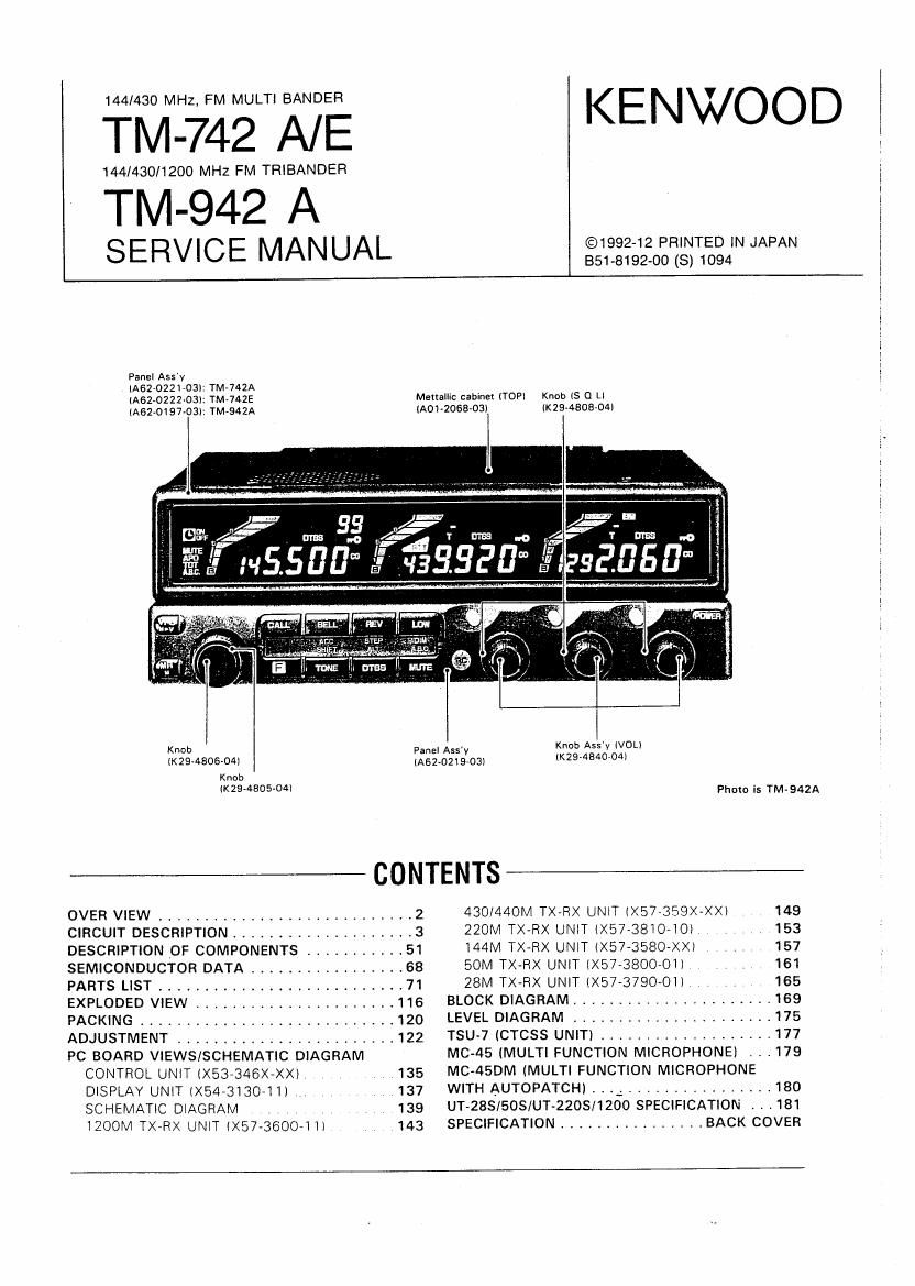
Kenwood TM 742 A Service Manual
This is the 167 pages manual for Kenwood TM 742 A Service Manual.
Read or download the pdf for free.
If you want to contribute, please mail your pdfs to info@audioservicemanuals.com.

Extracted text from Kenwood TM 742 A Service Manual (Ocr-read)
Page 2
TM-742 A/ 742 E/942 A
OVERVIEW "2
List of Destinations ,, :
Model Destination Destination code Model Destination Destination code
TM-742A North America K TM-942A North America K
TM-742A Canada P TM»942A Canada P
TM-742E Europe E TM-942A Other countries M
TM-74ZE Europe E2
TM-742E Europe E3
TM-742A Other countries M
TM-742A Other countries M2
Units for Each Model and Destination
Band Units
n" "am 9" "°- TM'nZAIE TM 942A UT-zas UT-sos UT-zzos UT-1200
K P E 52 E3 M M2 K P M M [50) M (50) K (50) M (10)
Control Unit X53-3460v11 o o 0
Control Unit XSS-SAGO-Zl o 0
Control Unit X53-3460-22 0
Control Unit X53646271 o 0
Control Unit X53-3462-72
Display Unit X54-3130-11 o o o o o o o o o o
ZBTX-HX X57-3790v0l o
50TX-RX X57-3800v01 o
lMTX-RX X57-3580~1 l o o o __
144TX-RX X57-3580~12 O o o o o o o
ZZOTX-RX X57-3810-10 o
MOTX»RX X57-3590-12 o o o
430TX-RX X57-359022 o o
430TX-RX X57~3592-72 O o o o
1200TX»RX X57-3600-1 1 o o o o
7
BAND UNITS
Any of the following optional band units may be installed
in the TM-742A/742EA
The same instructions apply for the Tri-Bander as for the
Dual-bender.
OPTIONAL BAND UNIT
TM-742A
UrS.A. Version UT»285 UT-SOS UT-ZZOS UT1200
TM»742A UT-ZBS UT-SOS UT-1200
TM-742E UT-ZBS UT-SOS UT~12OO
Page 58
TM-742 A/742 E/942 A
DESCRIPTION OF COMPONENTS
CONTROL UNIT (X53-346X-XX)
No. 1
Device number Use, function
Operation. condition. interchangeability
1C1 Microprocessor Refer to circuit description
ICZ SRAM memory
lC3 6VAVR 3 terminal regulator
13.6V 6V
(IN) #E-etoun
IC4 Address decoder For chip selector [llO expander)
|C5 Address decoder For chip selector ISRAM)
IC6 Serial time clock Refer to circuit description
|C7 Parallel - Serial converter IC Refer to circuit description
IC8 . Analog switch For DTHF receiver
lCQ Low frequency amplifier-adder MIC. amplifier DTMF modulation system adder
lC10 DTMF encoder Refer to the circuit description
lCl 1 DTMF decoder Refer to the circuit description
I012 Reset lC
IC13, 14 Serial data inverter buffer For serial data M
We E 33
m _. :101
3-DDLW
,EC
lClS Analog swrtch For switching during backup, (RD, WR)
IC16 Analog switch For switching during backup (CK)
IClOl lIO expander Refer to the circuit description
IC102 8V AVR 3 terminal regulator
i3 av av
(rm (our)
lClO3 Adder For internal speaker For level compensation
® Input llCtO4
|C104, 105 Low frequency amplification ® 13.8V @, ®, @, GND
Output liCioa-Band c, IClOS-Band A)
® Input lICiO4-Band C, |C105-Band A)
51
Page 62
TM-742 A/ 742 E/942 A
DESCRIPTION OF COMPONENTS
No. 2
Component Use/Function Operation/Condition[Compatibility
05-7 ln-band/out-of-band power SWilCh 06 OFF, 07 ON: ln-band reception; 06 ON, 07 OFF: Out-of-band reception
03 Second local oscillator bulfer Operation during reception 9.285 MHz
09 Squelch hysterisis switch ON while busy
Transmit/receive power switch
8V during reception 9 C
W during transmission Ln
1E'©- we on 2V while locked;
9 0.7V MI I k
C36L§C35 Q9 C3! . 'LCSD w 5 un 0c ed
E was was was rue I
010-014 .2 7:
0:2 a on "2
024 rh- .
M: N °'3 02
M)
I, R on car
1 I
010, 012. 013 OFF, 011, 014, 024 ON: During transmission
010, 012. 013. 024 ON, 011, 014 OFF: During reception
015-17 Inverter
Q13 Modulation system mute 0N during reception
019 CVline bulfer
020 HET output amplifier 28-29595 MHz, During transmission; 3633-38525 MHz: During reception
021 VCO 8V ripple filter
022 Middle (not for 10 W),
,_______
LOW Power swnch ,5, _ gm
DIO {floss
v.14}; Emu
{fia 022
©
(H: 7.5V '7 [Hz ov
M: 0v ,4, l M: 7.5V
L: 0V 'C " LL:0V /
023 AFC control Operation during transmissmn
025 and 026 OFF: During FM reception
025-026 AM/FM selection switch
025 and 026 ON: During AM reception
55