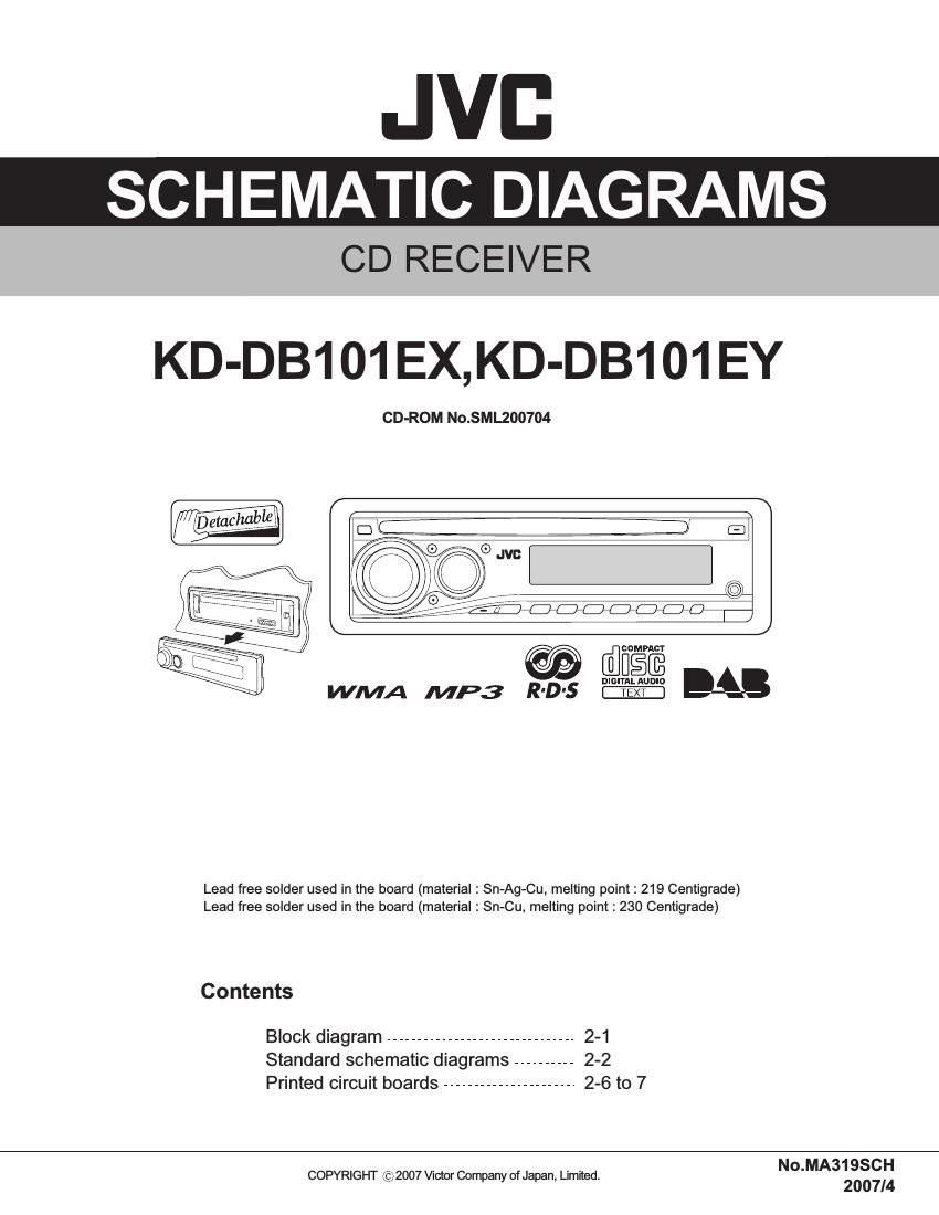
Jvc KDDB 101 EX Schematic
This is the 10 pages manual for Jvc KDDB 101 EX Schematic.
Read or download the pdf for free. If you want to contribute, please upload pdfs to audioservicemanuals.wetransfer.com.
Page: 1 / 10