Harman kardon avr 354 part 3

This is the 79 pages manual for harman kardon avr 354 part 3.
Read or download the pdf for free. If you want to contribute, please mail your pdfs to info@audioservicemanuals.com.

Page: 1 / 79
left right
harman kardon avr 354 part 3

Extracted text from harman kardon avr 354 part 3 (Ocr-read)


Page 1

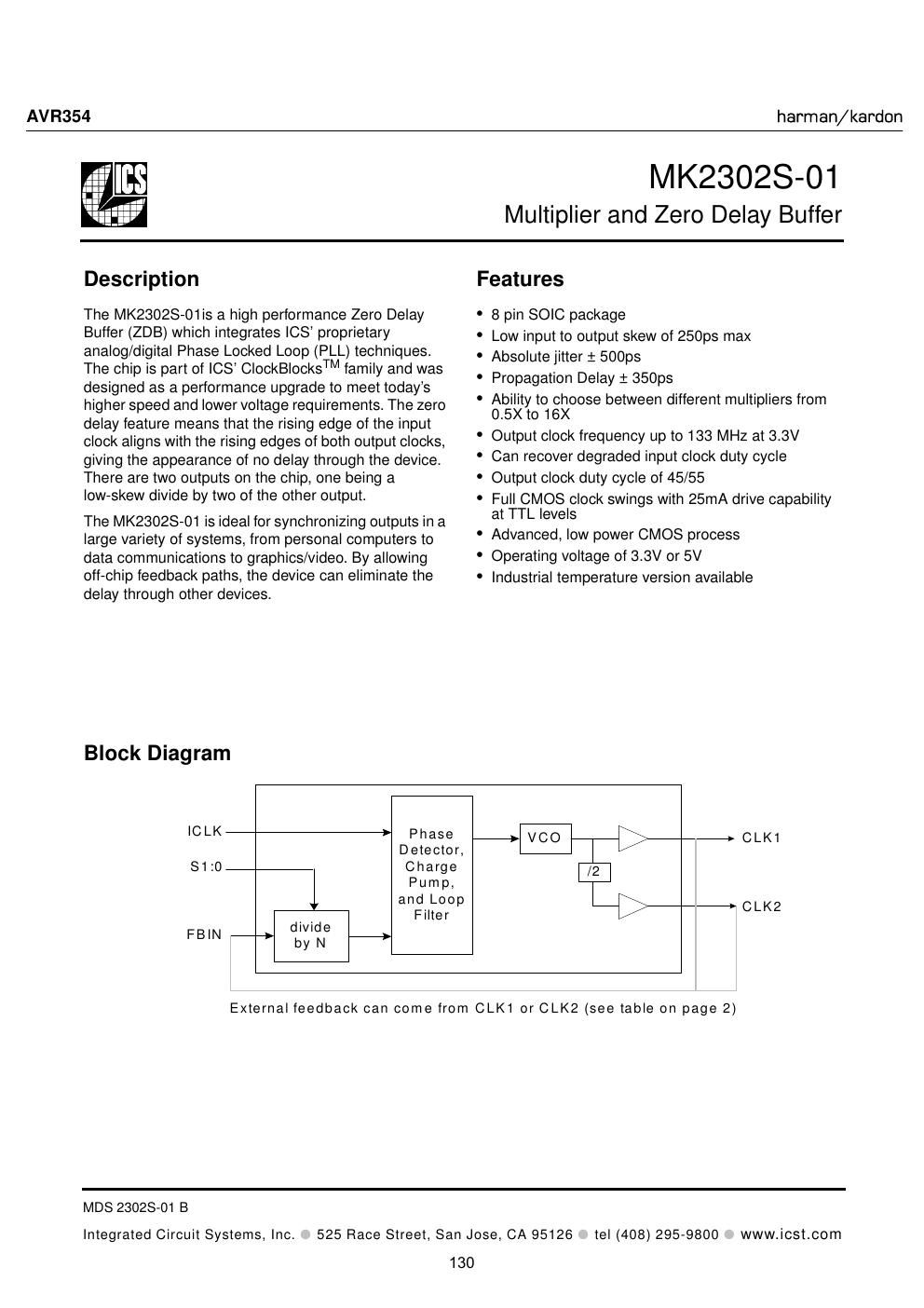
Multiplier and Zero Delay Buffer MDS 2302S-01 B Integrated Circuit Systems, Inc. - 525 Race Street, San Jose, CA 95126 - tel (408) 295-9800 - www.icst.com MK2302S-01 Pin Assignment Clock Multiplier Decoding Table 1 (Multiplies Input clock by shown amount) Pin Descriptions FBIN ICLK GND VDD S0 CLK1 CLK2 1 2 3 4 8 7 6 5 GND S1 1 2 3 4 8 7 6 5 8 pin (150 mil) SOIC FBIN S1 S0 CLK1 CLK2 CLK1 0 0 2 X ICLK ICLK CLK1 0 1 4 X ICLK 2 X ICLK CLK1 1 0 ICLK ICLK/2 CLK1 1 1 8 X ICLK 4 X ICLK CLK2 0 0 4 X ICLK 2 X ICLK CLK2 0 1 8 X ICLK 4 X ICLK CLK2 1 0 2 X ICLK ICLK CLK2 1 1 16 X ICLK 8 XICLK Pin Number Pin Name Pin Ty p e Pin Description 1 FBIN Input Feedback clock input. 2 ICLK Input Reference clock input. 3 GND Power Connect to ground. 4 S0 Input Select 0 for output clock per decoding table above. Pull-up. 5 S1 Input Select 1 for output clock per decoding table above. Pull up. 6 CLK1 Output Clock output per table above. 7 VDD Power Connect to +3.3V or +5.0V. 8 CLK2 Output Clock output per table above. Low skew divide by two of pin 6 clock. AVR354 harm an /k ar don 131

Page 2

Multiformat Video Encoder Six, 11-Bit, 297 MHz DACs ADV7342/ADV7343 Rev. 0 Information furnished by Analog Devices is believed to be accurate and reliable. However, no responsibility is assumed by Analog Devices for its use, nor for any infringements of patents or other rights of third parties that may result from its use. Specifications subject to change without notice. No license is granted by implication or otherwise under any patent or patent rights of Analog Devices. Trademarks and registered trademarks are the property of their respective owners. One Technology Way, P.O. Box 9106, Norwood, MA 02062-9106, U.S.A. Tel: 781.329.4700 www.analog.com Fax: 781.461.3113 ©2006 Analog Devices, Inc. All rights reserved. FEATURES 74.25 MHz 20-/30-bit high definition input support Compliant with SMPTE 274M (1080i), 296M (720p), and 240M (1035i) 6, 11-bit, 297 MHz video DACs 16× (216 MHz) DAC oversampling for SD 8× (216 MHz) DAC oversampling for ED 4× (297 MHz) DAC oversampling for HD 37 mA maximum DAC output current NTSC M, PAL B/D/G/H/I/M/N, PAL 60 support NTSC and PAL square pixel operation (24.54 MHz/29.5 MHz) Multiformat video input support 4:2:2 YCrCb (SD, ED, and HD) 4:4:4 YCrCb (ED and HD) 4:4:4 RGB (SD, ED, and HD) Multiformat video output support Composite (CVBS) and S-Video (Y/C) Component YPrPb (SD, ED, and HD) Component RGB (SD, ED, and HD) Macrovision® Rev 7.1.L1 (SD) and Rev 1.2 (ED) compliant Simultaneous SD and ED/HD operation EIA/CEA-861B compliance support Programmable features Luma and chroma filter responses Vertical blanking interval (VBI) Subcarrier frequency (F SC) and phase Luma delay Copy generation management system (CGMS) Closed captioning and wide screen signaling (WSS) Integrated subcarrier locking to external video source Complete on-chip video timing generator On-chip test pattern generation On-board voltage reference (optional external input) Serial MPU interface with dual I 2 C® and SPI® compatibility 3.3 V analog operation 1.8 V digital operation 3.3 V I/O operation Temperature range: 40°C to +85°C APPLICATIONS DVD recorders and players High definition Blu-ray DVD players HD-DVD players FUNCTIONAL BLOCK DIAGRAM R GND_IO VDD_IO 10-BIT SD VIDEO DATA 20-BIT ED/HD VIDEO DATA S_HSYNC P_HSYNC P_VSYNC P_BLANK S_VSYNC 11-BIT DAC 1 DAC 1 11-BITDAC 2 DAC 2 11-BIT DAC 3 DAC 3 11-BITDAC 4 DAC 4 11-BITDAC 5 DAC 5 11-BITDAC 6 DAC 6 MULTIPLEXER REFERENCE AND CABLE DETECT 16x/4x OVERSAMPLING DAC PLL VIDEO TIMING GENERATOR POWER MANAGEMENT CONTROL CLKIN (2) PV DD PGND EXT_LF (2) V REF COMP (2)R SET (2) ED/HD INPUT DEINTERLEAVE PROGRAMMABLE HDTV FILTERS SHARPNESS AND ADAPTIVE FILTER CONTROL YCbCr HDTV TEST PATTERN GENERATOR YCbCr TO RGB MATRIX G/B RGB ASYNC BYPASS RGB DGND (2) V DD (2) SCL/ MOSI SDA/ SCLK A LSB/ SPI_SS SFL/ MISO MPU PORT SUBCARRIER FREQUENCY LOCK (SFL) YUVTO YCrCb/ RGB PROGRAMMABLE CHROMINANCE FILTER ADD BURST RGB/YCrCb TO YUV MATRIX 4:2:2 TO 4:4:4 HD DDR DEINTERLEAVE SIN/COS DDS BLOCK 16× FILTER 16× FILTER 4× FILTER AGND V AA ADD SYNC VBI DATA SERVICE INSERTION PROGRAMMABLELUMINANCEFILTER 06399-001 ADV7342/ADV7343 Figure 1. Protected by U.S. Patent Numbers 5,343,196 and 5,442, 355 and other intellectual property rights. Protected by U.S. Patent Numbers 4,631,603, 4,577,216, 4,819,098 and other intellectual property rights. AVR354 harman/kardon 132