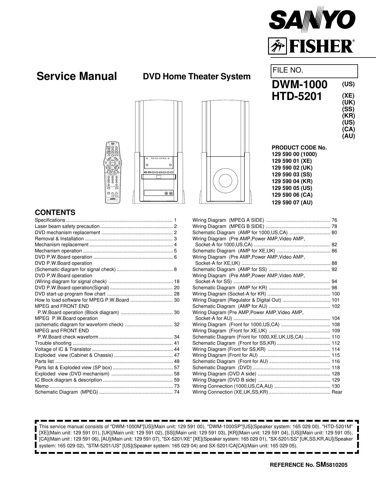
Fisher HTD 5201 Service Manual

This is the 63 pages manual for Fisher HTD 5201 Service Manual.
Read or download the pdf for free. If you want to contribute, please mail your pdfs to info@audioservicemanuals.com.

Page: 1 / 63
left right
Fisher HTD 5201 Service Manual

Extracted text from Fisher HTD 5201 Service Manual (Ocr-read)


Page 1

Service Manual

DVD Home Theater System

SA/WYO

frFlSHER

FILE NO.

DWM-1000
HTD-5201

PRODUCT CODE No.
129 590 00 (1000)
129 590 01 (XE)

129 590 02 (UK)

129 590 03 (SS)

129 590 04 (KR)

129 590 05 (US)

( I 129 590 06 (CA)

@

O O
| III II
( @
I
CONTENTS
Specifications ....................... . 1
Laser beam safety precaution. . 2
DVD mechanism replacement . 2
Removal & Installation .. . 3
Mechanism replacement .4
Mechanism operation .5
DVD P.W.Board operation .6

DVD P.W.Board operation

(Schematic diagram for signal check) ......................................... 8
DVD P.W.Board operation
(Wiring diagram for signal check) ............................................... 18

DVD P.W.Board operation(Signal).
DVD start-up program flow chart
How to load software for MPEG P.W.Board
MPEG and FRONT END


P.W.Board operation (Block diagram) ...................................... 3O
MPEGI P.W.Board operation
(schematic diagram for waveform check) ................................... 32
MPEG and FRONT END

P.W.Board check waveform ...................................................... 34

Trouble shooting
Voltage of IC & Transistor.
Exploded View (Cabinet & Chassis
Parts list ......................................

Parts list & Exploded view (SP box)
Exploded View (DVD mechanism)
IC Block diagram & description
Memo
Schematic Diagram (MPEG)

.57
.58

129 590 07 (AU)

Wiring Diagram (MPEG A SIDE) ..
Wiring Diagram (MPEG B SIDE) ..
Schematic Diagram (AMP for 1000,US,
Wiring Diagram (Pre AMP,Power AMP, deo AMP,

Socket-A for 1000,US,CA) ...........
Schematic Diagram (AMPforXE,UK) .
Wiring Diagram (Pre AMP,Power AMP,VIdeo AMP,

Socket-A for XE,UK) ........................
Schematic Diagram (AMPfor SS)
Wiring Diagram (Pre AMP,Power AMP,VIdeo AMP,

Socket-A for SS) ..............................
Schematic Diagram (AMP for KR)
Wiring Diagram (Socket-A for KR) .
Wiring Diagram (Regulator & Digital Out) .
Schematic Diagram (AMP forAU)
Wiring Diagram (Pre AMP,Power AMP,VIdeo AMP,

Socket-A for AU) ....................................................................... 104
Wiring Diagram (Front for 1000,US,CA) 108
Wiring Diagram (Front for XE,UK) 109
Schematic Diagram (Front for 1000,XE,UK,US,CA 110
Schematic Diagram (Front for SS,KR) . . 112
Wiring Diagram (Front for SS,KR) . . 114
Wiring Diagram (Front for AU) 115
Schematic Diagram (Front for AU) 116
Schematic Diagram (DVD) .. . 118
Wiring Diagram (DVD A side) . 128
Wiring Diagram (DVD B side) .. . 129
Wiring Connection (1000,US,CA,AU) 130
Wiring Connection (XE,UK,SS,KR)....


.101
102

(US)

(XE)
(UK)
(55)
(KR)
(US)
(CA)
(AU)

. Rear

f_______________________________________
I This service manual consists of "DWM-1000M"[US](Main unit: 129 591 00) "DWM-10008P"[US](Speaker system. 165 029 00). "HTD 5201M"

[XE]( (Main unit: 129 591 01) [UK](Main unit: 129 591 02) [SS](Main unit: 129 591 03), [KR](Main unit: 129 591 04), [US](Main unit: 129 591 05)
I [CA](Main unit: 129 591 06) [AU](Main unit:129 591 07) "sx- 5201/XE" [XE](Speaker system: 165 029 01) "sx- 5201/33" [UK 33, KR AU](Speaker
I sysIem: 165 029 02), "STM- 5201/US" [US](Speaker system: 165 029 04) and sx- -5201/CA[CA](Main unit: 155 029 05).

I.--I

REFERENCE No. SM5810205

Page 2

SPECIFICATIONS

Main unit with Main Speaker
Amplifier Section

US>

Main Amplifier

Continuous minimum sine wave RMS power output
per channel at 1kHz into 6 ohms with no more than
10 % total harmonic distortion . 30 Watts

Subwoofer Amplifier

Continuous minimum sine wave RMS power output at
100Hz into 6 ohms with no more than 10 % total
harmonic distortion 30 Watts

General

Output power
Total power : 90W
Main Amplifier: 30 X 2 (at 6 ohms, 10% distortion)
Subwoofer Amplifier : 30W (st 6 ohms, 10% distortion)

Input level and impedance:

VIDEO: VIDEO IN : 1.0 Vp-p (75 ohms)
AUDIO IN (UR): 600 mV/50k ohms
AUX/TV (L/R): 600 mV/50k ohms
Outputs:

MAIN SPEAKER (L/R): 6 ohms
SUBWOOFER: 6 ohms
PHONES:8-32 ohms (XE,UK,SS,KR,AU)
DIGITAL OUT: Optical
AV EURO CONNECTOR : For Euro-AV Cable (XE,UK)
COMPONENT VIDEO OUT: CB/CR: 0.7 Vp-p (75 )
Y: 1.0 Vp-p (75 )

MONITOR VIDEO OUT: 1.0 Vp-p (75 ohms)
AUDIO OUT (L/R): 600 mV (1 kohms)
S-VIDEO OUT: Y: 1.0 Vp-p (75 ohms)NTSC

Y: 1.0 Vp-p (75 ohms)PAL

C: 0.286 Vp-p (75 ohms)NTSC

C: 0.3Vp-p (75 ohms)PAL

DVD Video Player Section
Type: DVD/CD player
Playback standard : PAL or NTSC
Laser: Semiconductor laser. wavelength 650 nm
Laser output (Continuous wave max.)
1 mW (DVD)
0.5mW (CD)
Frequency range (digital audio):
4 Hz to 44 kHz (DVD fs: 96 kHz)
Signal to noise ratio: More than 105 dB
Harmonic distortion (digital audio): 0.003 °/o
Wow and flutter: Below measurable level

Main Speaker (magnetic shield)

Unit used: 10cm ( 4" diameter), Cone type
Maximum music power handling capacity: 60 Watts
Nominal impedance: 6 ohms

General

Power requirements: AC 120V, 60HZ (1000,US,CA)
AC 230V, 50HZ (XE,UK)
AC 230-240V,50HZ (AU)
AC 220V, 60HZ (KR)

Power consumption: 100 Watts
1.4W (standby mode)
Dimensions (W x H X D):Approx. 200(W) x 400(H) x 320(D) mm
Approx. 7.9" x 15.9" x 12.6"
Weight: :Approx.8.7 kg (19.4 lbs)

Main Speaker with Subwoofer (magnetic shield)
Main Speaker

Unit used: 10cm (4" diameter), Cone type

Maximum music power handling capacity: 60 Watts(peak)
Nominal impedance: 6 ohms

Subwoofer

Unit used: 13cm ( 5.1 diameter), Cone type

Maximum music power handling capacity: 60 Watts (peak)
Nominal impedance: 6 ohms

General

Dimensions (W x H x D): Approx 200(W) x 400(H) x 320(D) mm
Approx. 7.9" x 15.9" x 12.6"

Weight: Approx. 5.8 kg (13.2 lbs)

IMPORTANT INFORMATION

Because its products are subject to continuous improvement,
SANYO reserves the right to modify product designs and
specifications without notice and without incurring any obligation.

Specifications subject to change without notice.

Page 10

TROUBLE SHOOTING
(This is a basic trouble shooting.)

AUDIO PART

1. When time display OK and sound NG

or When S/PDIF 0K and anal

ogue NG.


Check DAC output
(10131 pin11/14).

OK

Tracking signal of
after DAC output.
Check MUTE signal.


Check (BCLK/
ASDATA/LRCLCIC131
pin 16/17/18).

Check lC131 pin1(27MHz)
and pin2(384FS).
Check lC131 power source
and peripheral circuit.
Check l0131 RESET/
control signal(pin6/7/8/9).


Check lC127
pin 105/106/107.

Check BCLK/ASDATA/
LRCLK signal line.
Check l0127 and

its peripheral.(|C127 NG)

Check IC127 peripheral.
(IC127 NG)

2. When time display NG and sound NG.

Exchange DVD:Loader.

OK

Loader NG.

Check IC127 peripheral.
(lC128 NG)

Check CD:CN810 pin2/3/4.

Check IC127 peripheral.
(IC127 NG)

Exchange loader.

Loader NG.

Exchange MPEG
p.w.board.

3. When S/PDIF NG and analogue OK.


Check optical module
and signal line.

Check lC127 peripheral.
(IC127 NG)

Check signal line
peripheralpattern
and parts.

4. When S/PDIF NG and analogue NG.

Check time display.

Check check 1

Check check 2

5. When pop noise (when usual operate.)

Check same output as
SPDIF and RCA.

YES

Loader NG

Check pop noise only
RCA output.

YES

Muting circuit trouble.
Check MUTE signal.

lC127 (MPEG) NG.

6. When pop noise (Power ONIOFF).

Check MUTE circuit.
(Normality 7)

Specity place of noise
generation.
Check timing with MUTE
signal and its peripheral.

Check MUTE circuit.

.42.

Page 27

IC BLOCK DIAGRAM 8t DESCRIPTION

- DVD LOADER section -

lC100 LA9702WL-MPB (Front End Processor forDVD Player)

iosr sun nan snzr

E

LPFI
LPF2

FH

EH

. .
iirra xoan

§ §
No Name Description No. Name Description
l RFN RF signal , input 4l RFOP RF 4 output
2 FIFP RF signal i input 42 CH RF bottom detection output
3 PDl Pickup signal input 43 PHl Resistance connection terminal to setting peak nold detect parameters
4 FD2 Pickup signal input 44 PH RF peak detect output
5 FD3 Pickup signal input 45 BOA BCA output
5 P04 Pickup signal input 46 DEF Detect output (H Detect detect)
7 FD5 Pickup signal input 47 DEFC Condenser connect terminal (or detect detect
a PBS Pickup signal input 45 TC Reslsiance connection terminal to setting deIeCl detect parameters
9 FD7 Pickup signal input 49 GND GND. (DTP pnage)
to P03 Pickup signal input so LFC Condenser connection terminal lor RF DC servo
ll PDQ Pickup signal input at CPOF Cnarge pump OFF terminal (H: OFF)
t2 VCC Power (Servo signal) 52 E002 RF equalizer setting terminal
l3 LDDI APCl output 53 TH Tracking hold (i-t Hold)
l4 LDSl APCl monitor voltage input 54 ECL2 RF equalizer setting terminal
l5 tum AFC2 output 55 VCC Power supply (DTP pnage)
ls LDSZ AFC2 monitor voltage input 56 5004 RF equalizer setting terminal
l7 GND GND (Sen/o signal) 57 XHTR Tracking, aottom detect band select (L High band)
to SOC Servo gain control terminal (RREC, FE, TE) 53 EQI4 RF equalizer setting terminal
19 FEBL Focus palance adjusting terminal 59 XQBH Bottom detect time constant select (L: Hign speed)
20 TEEL Tracking oalance adjusting terminal 50 E003 RF equalizer setting terminal
2l VGA FtF gain adjuslirlg terminal at EQSCT Equalizer select (H: 77 pin selection, L 52 pin selection)
22 BST Equalizer boost adjuslll'lg terminal 52 EQI3 RF equalizer setting terminal
23 FOST Focus oliset adjusting terminal 53 DPD/TE CPD, 3 oeam tracking select (H: DPD)
24 TOST Tracking oltset adjusting terminal 54 nFuz RF output
25 BCATH BCA tnresnold adjusting terminal as RFm RF output
26 REFl Standard voltage setting terminal 56 VCC Power supply (HF pnage)
27 SHEF standard voltage output loi servo signal 57 EQll RF equalizer setting terminal
23 RREC HeIIeCllon output as FF/TE 3 beam. pushrpull tracking select (L23 beam)
29 FE Eocus error output 59 Ecol RF equalizer setting terminal
30 TE Tracking error output 70 LDONZ APC2 Laser ON terminal (H. CN)
3i THC Condencer connection terminal to setting TE nold time constant 7l EQI2 RF equalizer setting terminal
32 we Woople output terminal 72 LDONI APCl Laser ON terminal (H. ON)
33 ISET Resistance connection terminal to setting BPF center lrequency 73 E002 RF equalizer setting terminal
34 wot Pushrpull signal input 74 GND GND. (RF phage)
35 woo Fushrpull signal output 75 EOL1 RF equalizer setting terminal
as TEC TE gain setting terminal lor 3 oearn 7e RFSCT RF input select (H RF dilierential input, PF error)
37 TEN TE gain setting terminal lor 3 oearn 77 Eom RF equalizer setting terminal
35 CP Heslslance to setting cnarge pump gain Condenser connection terminal 73 CAO Customer Amplilier output
39 BM Resistance connection terminal to setting bottom nold detect parameters 79 PREF Standard voltage output (tor Pickup)
4o RFCN HFr output so CAN Customer Amplilrer input

.59.

Page 54

SCHEMATIC DIAGRAM (AMP for KR)

«g S m
E: 3:;
(2422 (Luna
E L-EN
t
rva
R-cu
mm m 1 is
tAVAJmMJm m k gel
Mg
m an
m. vucun .._
.m>-o H
mm»
H 3
mac mama:
KLC753424 can:
i a a an 7
s MAM. s 7 a a In 11 i2 13 u 15 Is :7 In 13
a :fluistuismflsfl
3-6
3-6
1a
'0 i
2 2


a 5 FAN

uflfi Kfflifia

Ari/own


v

9.02? man 2.2x

Futmtim A mam. A Wtcuthz A

J

.J

pry/ems;

RtEE


ac mum:


4th g

cm57
mums-mm


t l :2 mass *
WM: . a imam PRODUCT SAFETY
X NOTICE
Each precaution in this manual
should be iollowed during
iAV5¥§%§a._ V servicing. Components
m 22* $533132;
«av c 1 .
m" "3 +5v Ev: schematic diagram designated
1L; < m p a components in which salety can
* < ' -37? H2V be of special significance. When
replacing a component identified
_ by A , use only the replacement
7 parts designated, or parts wtth

é

XX
E5

nu ma ms
an M71)

Autism

FL
FLL

TCI PT

the same ratings of resistance,
wattage or voltage that are
designated in the parts list in this
manual. Leakagercurrent or
resistance measurements must
be made to determine that
exposed parts are acceptably
insulated from the supply circuit
before returning the product to
the customer.


ascraxc mum _

EM 0
nmiiwu mu

This is a basic schematic diagram.

.99.