Ampex ATR 100 Operation Maintenance

This is the 146 pages manual for Ampex ATR 100 Operation Maintenance.
Read or download the pdf for free. If you want to contribute, please mail your pdfs to info@audioservicemanuals.com.

Page: 1 / 146
left right
Ampex ATR 100 Operation Maintenance

Extracted text from Ampex ATR 100 Operation Maintenance (Ocr-read)


Page 1

0

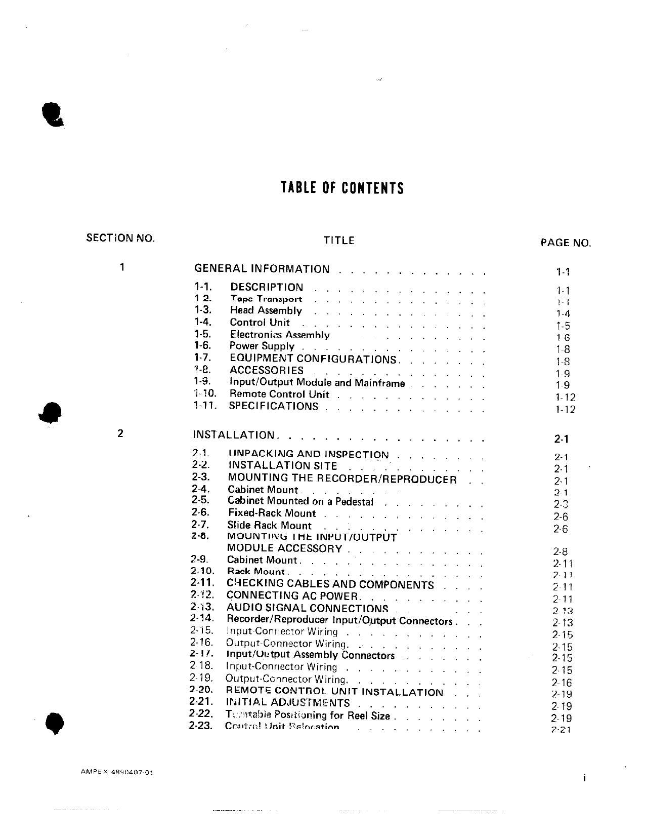
SECTION NO.

AMPEX 489C407'01

GE
11.
12.
1-3.
1-4.
1-5
16
17.
18.
1-9.
1.1
1

0
1.

'd

TABLE OF CONTENTS

TITLE

NERAL INFORMATION

DESCRIPTION

Tape Transport

Head Assembly

Controi Unit

Electronics A<=emhly

Power Supply . . .

EQUIPMENT CONFIGURATIONS.
ACCESSORIES . . .
Input/Output Module ancI Mainframe ,
Remote Control Unit .
SPECIFICATIONS .

INSTALLATION.

?.1

2-2.
2-3.
2-4.
2-5.
2-6.
2-7.

IINPACKING AND INSPECTION .
INSTALLATION SITE . .

MOUNTING THE RECORDER/REPRODUCER
Cabinet Mount , .

Cabinet Mounted on a Pedestal

Fixed- Rack Mount .

Slide Rack Mount . .

MOUNTING THI: INPUT/OUTPUT
MODULE ACCESSORY.

Cabinet Mount.

Rack Mount . .

CHECKING CABLES AND COMPONENTS
CONNECTING AC POWER. . .

AUDIO SIGNAL CONNECTIONS
Recorder/Reproducer Input/Output Connectors .
Input Connector Wiring , . . .
Output Connector Wiring.

Input/Output Assembly Connectors

Input Connector Wiring

Output Connector Wiring

REMOTE CONT ROI UNIT INSTALLATION
INITIAL ADJLI TMENTS .

T; w big Posrtioning for Real Size .

:I .Inil Iifiimzatinn


PAGE NO.

_l
.a

Aeéamwdomtné~¥

a_._._-_._._._4_.__t
MM

d

N" NNNPNNN N
-IOU 0303;.J_I_._I_.

N .. '3

MNNNNNNNMNwNM
figddgga_a_tg.go_.
econommmo-Immwmd-t

Page 2

SECTION NO.

TABLE OF CONTENTSIGunUnueM

TITLE

INSTALLATION (Continued)

2-24. SpooIrSpeed Selection . .
2-25. Play/Edit Mode Lockout .
226. Record Mode Lockout . .
2-27. Tape Timer Display Selection .
2-28. Minutes, Seconds and Tenths of Seconds Display
129. Hours Minutes, and Seconds Display . .
2-30. PU RC Operation Selection . . .
2-31. INITIAL CHECKOUT PROCEDURE
2 32. FACTORY SHIPPED
OPERATIONAL CONFIGURATION .

2~33. CHECKING OPERATING LEVEL .
OPERATION . , . .
3-1. CONTROLS AND INDICATORS .
3-2. PRE- OPERATING PROCEDURES.
3-3. OPERATING PROCEDURES .
3-4. Recording

'5. rant Winding
3-6. Reproducing .
3-7. Tape Timer Operation.
38. Sel Sync FIInMinn
3-9. Editing.
3-10. Spooling . .
311. Remote Control Operation .
3-12. PURC Operation . .
313, Editing Procedures .
3714. Insert Edit

THEORY OF OPERATION.

4-1.

4.2.
4.3.
4-4.
4-5.
4-6.

FUNCTIONAL DESCRIPTION
OF TAPE TRANSPORT

BLOCK DIAGRAM FUNCTIONAL DESCRIPTION I

Thread Mode . .
Reproduce Mode

Record Mode
Spool Mode .

PAGE NO.

2723
777'?
2724
2724
2-24
2725
2726
2729

pp
(ow
6...

-n._l-l_|_.\._a_1_|_|._l_|-t._a-d .-

CDUTUIUIJfiLQCAJmfiA-I-I

wwwwwwwwwuwwww

P
_.

4-1
4.1
4-2
4.2
4.2
4.2

AMPE X 4890407 01

Or

Page 13

TABLE NO.

_._i_._\
bWN-l

5.5

576
5-7

AMPtX 4?}8040/ Ul

lIST OF TABLES

TITLE

Floctrnning Accnmhly Printed \Miring Accemhliuc
Optional Equipment

Accessory Equipment .

Specifications .

Power Jumper Positions . .
Connector Ji3 Channel/Signal Identification
Channeisi and 2..
Connector Jl4 Channel/Signal identification
Channels 3 and 4.

Factory Shipped Operational Configuration

Tape Transport Controls and indicators .

Recorder Control Panel Transport Controis and indicators
Recorder Control Panel

Signal System Controls and Indicators .
Input/Output Module Accessory, Controls and Indicators .
PU RC Edit Delay Times .

Command Signal Abbreviation.
Phase Comparator Output Logic States
Tape Speed Reference Frequencies.
Capstan Servo FET Switch Control.

Channel 1 Signal Mode Selection Output Signal Logic Slates

Speed Jumper Placement and Bias Switch Setting,
Audio Control PWA No 5 . .

Preset Equallzatlon Network Settlngs .

Counter Data Word Format

Overall Test and Maintenance Equment fieqmrements.
Lubricants Used on Recorder/Reproducer .

Reproduce Frequency Response Tolerances

Amplitude Correction Factors for Setting Operating chcl
when using Full- Track Alignment Tapes on 2 Track

or 4 Track Systems .

Capacitor Values for Passive Edualization

of High Frequency Turnover

Relatlve Operatlng Levels.

PADN ET PWA Alignment Controls.

PAGE NO.

_\_.H_I
44
comm

All

478
49
4'28

438
4746
4756

@9514.
-\\l__

516

5-18
5-21
5724

xiii

Page 28

Table 1-3. Accessory Equipment (Continued)

DESCRIPTION

AMPEX PART NO.

Remote Control Unit, FourrChannel 7 includes 25100! (7 62 mi
anlivc L'nUl'e allU connector
Optional Scrape Flutter Idler (not interchangeable With furnished idler)
TworWay Extensrtm Accessory Connector Assembly
Neise Reduction Switching Interface (Dolby/08X Switcherl
Flux Loop
Flux Loop Equalizing Amplifier
ATR~100 Spare Parts Kits
A" Level Spares
E" Level Spares
Full Track
2 Track
A Tmrk
"C" Level Spares
1/4-inch (6.4 mml Tape
1/2 inch (12.7 mmi Tape
V5710 Variable Speed Oscillator
VS-10 Variable Speed Oscillator with Readout
Euii Code Generator
Edit Code Reader

4010264
4030402-AB
4020432
4020433
4020423
4020424

1385874

138587501
138587502
1305075-03

1385876-01
IJUbU/UUZ
4010217-07
4010217708
4010166
4010187

Table 1 4. Specifications

_ in, Widthc:

\1/4 inch (6.4 mm) i0) fullrtrack and Zrtrack, Zchannel systems, 0.075 Inch (1 9 mm) track Width.

\\ 1/2 inch (12.7 mml for 4-track systems, 0070 (1.8 mm) track width.
Tape Speeds:

375 m/s (9.5 cm/s)

7.5 in/s (19.05 cm/sl

15 m/s (38.1 cm/s)

3O in/s (75.2 cm/s)

(anv two sueeds mav hp. se(F(rmll
Reel Size:

27inch to 144F101 diameter (50 mm to 355 mm?

Raul Typo:
NAB, EIA (Cme'l

Al/lpzv «pom/37 m

Page 38

.-6. Fixed-Rack Mount

in the fixed-rack configuration (Figure 2-6), the
electronics assembly chassis is separated from the
transport and is mounted directly beneath the
transport so that the printed wiring assemblies
(PW/As) tace forward toward the operator. This
equipment is mounted in a standard 19-inch rack
or in a custom cabinet as follows:

1. At the top of the transport, remove the
rear overlay panel (six screws) shown in
Figure 272.

2. Locate the three transport mounting holes
(Figure 2-3) that are used to mount the
transport.

3. Mount the transport onto the rack or custom
cabinet using three appropriate size screws,
depending on the type of rack or cabinet.

4. Mount the elprtmnicc frame furnished in
the fixedrrack mount kit directly beneath the
transport using four appropriate-size screws,

. depending on the type of rack or cabinet.

5. Remove the front cover from the electronics
assembly and remove all PWAs from the
inside of the assembly.

CAUTION

FOR THE FOLLOWING STEPS, DO NOT
PUT EXCESSIVE STRAIN ON CABLES
OR CONNECTORS. CLIP CABLE TIE
DOWNS AS REQUIRED,

6. From the inside of the electronics assembly
chassis, remove three 682 screws that secure
the head cable assembly to the electronics
chassis.

7. Carefully unhook electronics assembly chassis,
from transport and rotate chassis so that
interior of chassis faces forward. Slide chassis
into flanges of electronics frame.

8. Secure electronics assembly chassis to elec-
tronics frame With four 682 screws and a
lockwasher under screw head.

9. Reinstall PWAs removed in step 6.
2-7. Slide Rack Mount

In the slide-rack mount configuration (Figure 1-9),
the recorder/reproducer is mounted on a pair of
slides (Figure 277) that are attached to a 19-inch
(48.26 cm) rack that has both front and rear rack
mounting members. When installed, the recorder/
reproducor may be pulled forward on the slides
and rotated 90° upward to permit easy access to
the PWAs within the electronics assembly. The
slides enable the transport to be extended far
enough from the rack to permit 90° rotation of
the transport when 14inch (35.56 cm) reels are
mounted on the transport.

WARNING

THE RACK USED TO MOUNT THE
RECORDER/REPRODUCER MUST BE SE-
CURELY FASTENED TO THE RACK
MOUNTING SURFACE TO PREVENT THE
RACK FROM TIPPING FORWARD WHEN
THE RECORDER/REPRODUCER IS EX-
TENDFD FORWARD

All parts and hardware for mounting the recorder/
reproducer are furnished in the slide-rack mount
kit, Ampex Part No. 4010253. Mount the dis
assembled slide-rack mount kit parts as follows:

1. At the top of the transport, remove the rear
overlay panel (six screws shown in Figure
2-2).

2. Locate the six transport mounting holes
(Figure 2-8) that are used to mount the
transport to the pivot bracket.

3. Fasten each pivot bracket to the rear of the
transport using three 10-32 X 3/4 inch long
socketehead screws with a no. 10 split washer
under each screw head (do not use flat
washers). Note orientation of pivot bracket
flange shown in Figure 27.

4. It slide-rack mount parts are not separated,
press release hmmn nn sirlp nf inngr slide
member (Figure 27), and remove inner slide
member from middle slide member.

AMPEX 4890407401

3

Page 83

.84. :15-Vdc Regulator. A :15Vdc zener
diode regulator is used to power the input/output
module assembly. Power in the form of :24 Vdc
is furnished from the ATR-TOO and is applied to
seriespass transistors 07 and 08, which are con»
nected as emitter followers. The output voltage at
the emitters of 0/ and 05 is determined by
zener diodes VRl and VR2, which are connected
between the base and ground of Q7 and 08,
respectively.

4-85. Tape Timer
Functional Description

The tape timer displays in hours, minutes, and
seconds the elapsed time that the tape has moved
at the selected speed from a zero reference estab
lished by pressing the RESET pushbutton switch
on the control unit. The tape timcr contains a
counter and assomated arithmetic logic to detect
the relative tape position and provide a timer
multiplexed. binaryrcoded decimal lBCDl output
for the display of the tape position in hours,
minutes, and seconds of play/record time at the

lected tape speed, The tape timer receives a tape
direction signal from the control unit, a selected
speed signal from the tape transport, and pulses
from a tape-driven tachometer (tach) on the tape
transport. The tape timer counts the number of
tach pulses received, converts the length of tape
represented by the tach pulses to record/play time
at the selected speed, and adds or subtracts the
time represented by the tape motion from the
current time being displayed, depending on the
direction of tape motion. The tape timer sends
five binaryvcoded decimal digits to the display on
the control unit. To minimize the number of inter
connecting leads between the tape timer and the
control unit, the five digits are transmitted serially
over a common 47bit bus to a BCD to7 segment
decoder in the control unit. The output of the
BCD»tor7 segment decoder is sent in parallel to
five 7-segment display indicators that comprise the
b-digit display on the control unit. Five digit select
lines are also sent to the control unit. The digit
select lines identify the current digit being sent
from the tape timer and enable the corresponding
one of five 7-segment display indicators.

4-54

4-86. Tape Timer Circuit Details

The tape timer circuitry is principally located
on transport control PWA No, 7. The display
and ancillary BCD-to-7-segment encoder are
located on the control unit, Figure 425 is a
simplified block diagram of the tape timer, and
drawings 4840397 and 4840396 are the schematic
diagrams, respectively.

4-87. Tape Timer Display. The tape timer dlSr
play is contained on the control unit assembly and
consists of five 7~segment light emitting diode
(LED) display indicators {Al through A5 on con
trol unit PWA V0. 1), five driver transistors (01
through (15 on PWA No. 1), and a BCDrIO'T
segment encoder (A3 on PWA No. 2). The serial
stream of binaryrcoded decimal digits from the
tape timer logic on PWA No, 7 are sent to the
BCD-tolsegment decoder A3 located on the
control unit PWA No. 2. The binaryrcoded decimal
digits are sent via 4 lines; BCDVA, BCDVB, BCDVC,
BCDVD. The BCDrtor7-segment decoder A3 pro
vides a logic low (ground) to the segments required
to form the digit, which is sent in BCD via BCDVA
through BUD-l), on the display.

The seven lines that comprise the output of the
bUUrto-rsegment decoder A3 are sent to the
control unit PWA No. l, where they are connected
in parallel to each of the corresponding segments
on the five 7 segment displays, A1 through AS.
Each of the five 7-segment displays consists of
seven light emitting diodes with common anodes.
Selection of the 7»seoment pattern corresponding
to the digit sent via the BCDVA through BCDVD is
accomplished by applying a positive 5 volts llogic
high) to the anode of the selected 7-segment dis
play and keeping the anodes oi the other 7rsegment
displays at ground (logic low). The digit selection
signals DSVi through D875 from the tape timer
circuits on the trai'ispoit logic FWA Nu. 7, via
transistor switches, provide a positive 5 volts to

the anode of 7-segment display Al through A5,
resnpctivoly When a digit CDlQLt ling 3ch MW
(0 Vdc), the associated transistor switch conducts
and provides a positive 5 volts to the anode of
the corresponding 7rsegmeiit display. Since only
one digit select line goes low at a time, the remain
ing transistor switches are not conducting, and the

AMPE X 4890407 Ci

Page 140

driver Qi7/VR5. The output of the driver ampli
fier 018/019 also goes to the erase voltage status
switch 016 which supplies a low to the erase
voltage status line (EVS) when the erase voltage is
present at the output of driver amplifier 018/019.

When the channel is not in the record mode, the
144 kHz from the master erase bus through resistor
R83 is shunted to ground by erase ramping switch
014, and erase head relay K2 is derenergized,
which opens the circuit to the winding of the
erase head.

4-76. Reproduce Circuits. The reproduce cir-
cmts pI'OVlCle amplification, selection, and post
equalization of the playback signals. Figure 4-22
shows a simplified block diagram of the reproduce
circuits.

As shown in Figure 4722, the reproduce circwt
contains the sol sync hood preamplifier, reproduce
head preamplifier, and reproduce equalizer amplir
fier. The reproduce head preamplifier receives the
lavback signal from the reproduce head and is
located on the main audio PWA. The sel sync
head preamplifier receives the playback signal from
the sel sync winding on the record head and is also
located on the audio main board Ihe outputs of
the two head preamplifiers go to the standard
PADNET assembly where, via the individual sel
sync and rcproducc gain controls, the signal is
applied to the summing pomt at the input to the
reproduce equalizer amplifier through the sel sync
and reproduce switching FETs. The reproduce
equalizer amplifier provides post-equalization of
the selected playback signal. The output of the
reproduce equalizer amplifier IS fed back, via speed
selected equalization and compensating networks
located on the PADNET assembly, to the summing
point at the input of the reproduce equalizer
aiiiplifici. The output of iepiuduue equalizer
amplifier is also sent to the audio output ampli»
fier via erase frequency trap 03/L1 and input
resistor; FIB/R9.

The signal from the sel sync winding on the record
haarl is rnnnprtenl thrnugh capacitnr C31 to the
input of the sel sync preamplifier. Sel sync winding
shunt switch 06 at the input to the sel sync prey
amplifier consists of transistor switch 06, operating

4-48

in the inverted mode which shorts out the sel sync
winding during record. Transistor switch C16 is
controlled by the output of the bias ramping con
trol amplifier A78 in the control logic. Resistor
R33. in parallel with the input to the sel svnc prev
amplifier, provides damping of the sel sync winding
at resonance. The sel sync preamplifier consists of
transistor 05 and amplifier A4 arranged as a
feedback-controlled voltage amplifier. The signal
from the sel sync winding of the record head is fed
to the base of transistor 05, The output from tran-
sistor 05 is fed to the iiivcitii'ig input of aiiiplifiei
A4. Part of the output from amplifier A4 is fed
back to the emitter of transistor 05 via network
C11/C12/C18/l 2/R15-R17 The norwnrlr fnrmorl
by R15, R 16, and C18 provides additional negative
feedback to attenuate mid-range and high fre-
quencies, thereby providing a low frequency boost
in the output of sel sync preamplifier to compen»
sate for the inherent rollroff in the reproduce signal
from the sel sync windings. Resistor R17, in con
Junction with CZB/fi37, sets the lowrtrequency
gain of the sel sync head preamplifier. Capacitor
C12 and inductor L2 in this network form a series
resonant trap at the bios frequency. The output of
the sel sync head preamplifier A4, via resistor R49,
goes to the unequalized sel sync output at the
PWA-edue connector. From here the signal is routed
to connector J13/J14. The output of the sel sync
head preamplifier, via capacitor C13, goes to the
sync gain control R3/R4 located on the PADNET
assembly,

in a similar manner, the audio from the reproduce
head is amplified by the reproduce head preampli»
fier consisting of operational amplifier A3 and
transistor 04 arranged to form a feedback con,
trolled amplifier. The audio from the reproduce
head goes to the base of transistor 04 via inductor
L3 which provides RFI filtering. Head damping
network R36/R34, in parallel with the audio input
to the base of transistor 04, provides adjustable
damping of the high-frequency head resonance.
The output from amplifier A3 is fed back to the
input of transistor 04 via RC network C24/R31.
This RC network, together with RC network
CZ7/R32. sets the ac gain of the reproduce head
preamplifier. Another RC network formed by
R23/C23 limits the open loop gain of operational
amplifier A3.

AMFEX 4890407 01