Akai GX 266 Mk2 Service Manual
This is the 62 pages manual for Akai GX 266 Mk2 Service Manual.
Read or download the pdf for free.
If you want to contribute, please mail your pdfs to info@audioservicemanuals.com.

Extracted text from Akai GX 266 Mk2 Service Manual (Ocr-read)
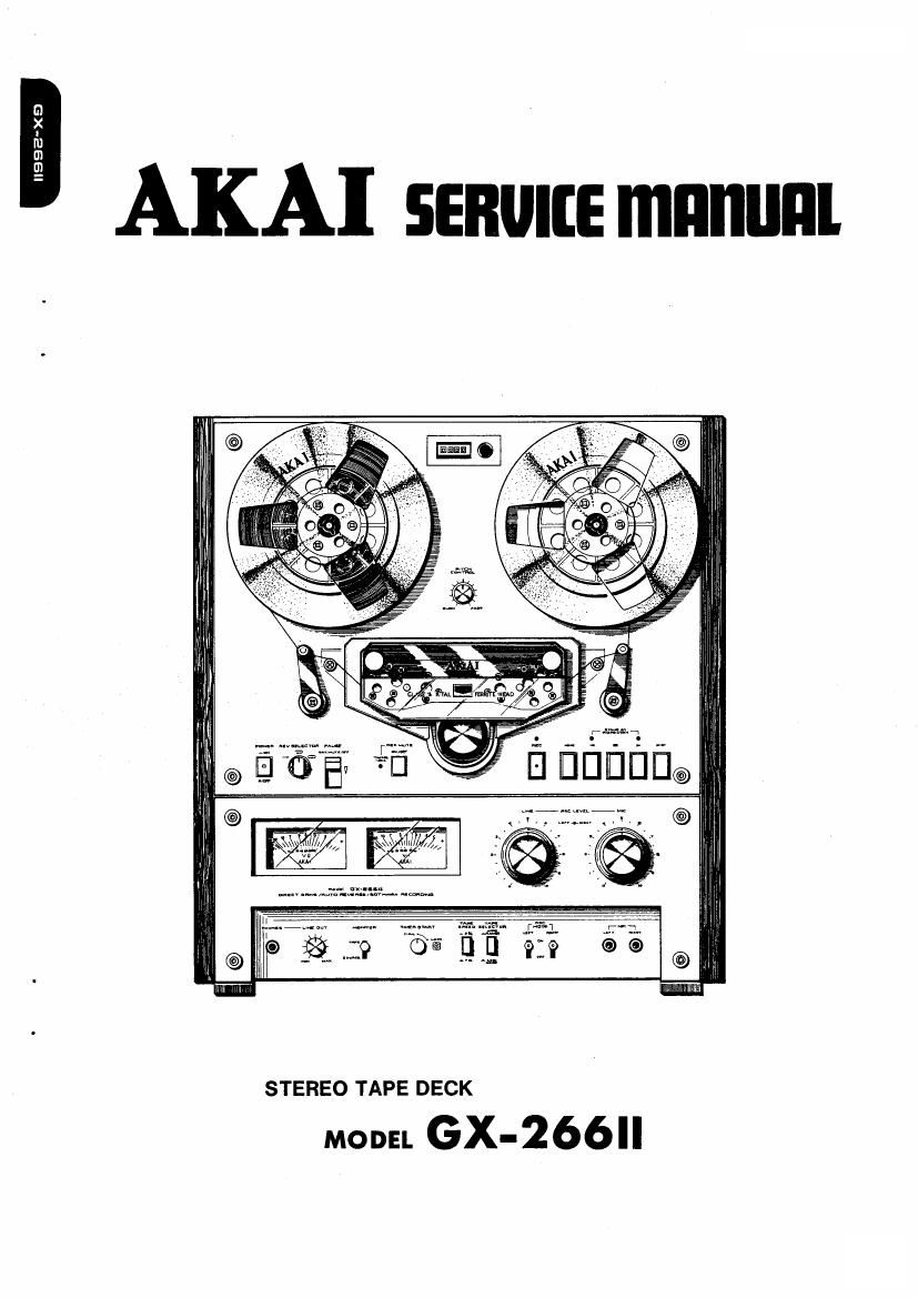
Page 2
STEREO TAPE DECK
MODEL GX'2 6611
ALSO APPLICABLE TO BLACK PANEL MODEL
SECTION I SERVICE MANUAL .................... 3
SECTION 2 PARTS LIST .......................... 39
SECTION 3 SCHEMATIC DIAGRAM ................ 63
Page 4
I. TECHNICAL
DATA
TRACK SYSTEM
REEL CAPACITY
TAPE SPEED
WOW & F LUTTER
FREQUENCY RESPONSE
4 track 2 channel stereo/monaural system
Up to 7" reel
19 cm/s i 0.8% (7-1/2 ips)
95 cm/s i 1.0% (3-3/4 ips)
(Pitch control : t 6%)
Less than 0.03% WRMS, 009% DIN 45500 at 19 cm/s
Less than 0.04% WRMS, 0.11% DIN 45500 at 95 cm/s
30 to 26,000 Hz 1 3 dB at 19 cm/s (WR Tape)
30 to 19,000 Hz i 3 dB at 9.5 cm/s (WR Tape)
DISTORTION Less than 0.5% (at 1,000 Hz 0 VU)
SIGNAL TO NOISE RATIO Better than 62 dB DIN 45500 at 19 cm/s
ERASE RATIO Better than 70 dB (at 1,000 Hz)
CROSS TALK Better than 40 dB (at 1,000 Hz)
CHANNEL SEPARATION
BIAS FREQUENCY
Better than 55 dB (at 1,000 Hz)
100 kHz
HEADS (6): Two GX recording heads, Two GX playback heads
Two erase heads
MOTORS (3): One AC servo motor for capstan drive
F.F & RWD. TIME
Two AC eddy current motors for reel drive
90 sec. using 360 m (1,200 ft.) Tape
OUTPUT JACKS Line (2): 0775 V (0 VU)
Required load impedance: more than 20 kohms
Phone (1): 100 mV/8 ohms
INPUT JACKS Microphone (2): 025 mV
Required microphone impedance: 600 ohms
Line (2): 70 mV
Input impedance 100 kohms
DIN JACK Input: 2.0 mV
Input impedance 10 kohms
OutpUt: 0.3 V
DIMENSIONS 440 (W) x 470 (H) x 250 (D) mm (17.4 x 18.5 x 9.8)
WEIGHT 18.7 kg (41.3 lbs)
POWER REQUIREMENT
POWER CONSUMPTION
100V 50/60 Hz switchable for JAPAN
120V 60 Hz for US & Canada
220/24OV switchable, 50 Hz for European countries & Australia
110/120/220/240V, 50/60 Hz switchable for other countries
65 W for JPN, CSA Model
90 W for U/T Model
* Specifications determined with Akai LN-150-7 or SCOTCH #211 tape unless otherwise noted.
For improvement purposes, specifications and design are subject to change without notice.
Page 17
2) Explanation of the circuit operation
(Refer to Figs. 8, 9)
The velocity signal obtained from the motors
frequency generator is shaped into a waveform in
the period of "T proportionate to the velocity
as in (a) on collector TR6. This signal is differen-
tiated and enters TR7 base. This makes TR7s
collector output as in (c) and turns ON TRIO
during the time of the negative pulse.
Meanwhile TR8 base is supplied with a waveform
like (d) and when it reaches the threshold level,
TR8 is turned on. A waveform (c) with pulse
width t1 " is obtained from the collector. During
the time T that TRS is ON, TR9 base electric
potential decreases to turn ON.
Consequently, TRll base electric potential in-
creases and TRll is also turned 0N for the time
n".
When the period T varies with the velocity,
the pulse width t1 varies according to TR8s
threshold level. But when TRIO is on, it is con-
stant due to the time constant. So that by using
the period that TRIO is ON as the standard pulse,
the pulse width t1 " is constant regardless of the
velocity. (g) and (h) show the ON and OFF
condition of TRlO and TRll. When the electric
charge that was charged to C17 is discharged
during the time TRll is ON t, , a signal voltage
of e" proportionate to the velocity can be
obtained. Next, with e as its basis, C17 is
charged during the limited time of the standard
pulse width t2, and by the charging voltage
e the charging is stopped
The voltage is then held until the next standard
pulse.
This voltage e is supplied to the TR12 base and
a servo signal E" is obtained. This servo signal
E controls TR] and drives the motor. As shown
above, since t1" and t2 are small, servo signal
ripples are made small and a near direct current
servo signal is obtained.
In addition, the time constants of the smoothing
circuit can also be made small that phase lag factor
can be minimized.
l8