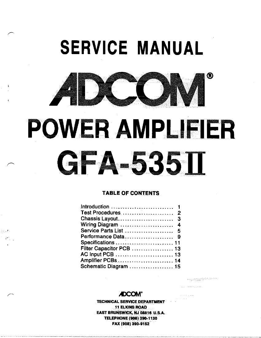
Adcom GFA 535 II Service Manual
This is the 17 pages manual for Adcom GFA 535 II Service Manual.
Read or download the pdf for free.
If you want to contribute, please mail your pdfs to info@audioservicemanuals.com.

Extracted text from Adcom GFA 535 II Service Manual (Ocr-read)
Page 1
SERVICE MANUAL
ADCOM®
POWER AMPLIFIER
GPA-535]]
TABLE OF CONTENTS
Introduction .......... . ................ 1
Test Procedures ...................... 2
Chassis Layout ........................ 3
Wiring Diagram ....................... 4
Service Parts List ..................... 5
Performance Data ..................... 9
Specifications ......................... 1 1
Filter Capacitor PCB .................. 13
AC Input PCB ......................... 13
Amplifier PCBs ........................ 14
Schematic Diagram ................... 15
DOOM
TECHNICAL SERVICE DEPARTIIENT
1 1 ELKINS ROAD
EAST BRUNSWICK, NJ 03316 USA.
TELEPHONE (908) 390-1 1 30
FAX (908) 390-9152
Page 2
INTRODUCTION
This service manual is intended to assist trained and qualified technical personnel in verifying the performance at,
adjusting. and repairing the ADCOM GFA-535H power amplifier. The procedures described here are not intended for
persons unfamiliar with the appropriate safety and test procedures.
WARNING
THERE ARE POTENTIALLY LETHAL VOLTAGES WITHIN THE GFA-SSSII AMPLIFIER WHICH WILL BE
ACCESSIBLE ONCE ITS TOP COVER IS REMOVED. DO NOT ATTEMPT FAMILIARIZATION, INSPECTION
OR ANY PROCEDURE WHATSOEVER UNLESS YOU HAVE DISCONNECTED THE GPA-535 FROM THE
WALL AC OUTLET OR OTHER SOURCE OF AC POWER AND THE POWER-SUPPLY CAPACITORS ARE
COMPLETELY DISCHARGED. PLEASE TAKE NOTE THAT THE POWER-SUPPLY CAPACITORS TAKE AS
LONG AS 5 MINUTES TO DISCHARGE. THESE INSTRUCTIONS ARE PROVIDED FOR USE ONLY BY
COMPETENT TECHNICAL PERSONNEL. DO NOT UNDERTAKE ANY SERVICE PROCEDURES IN THE
GFA-535II UNLESS YOU ARE TECHNICALLY QUALIFIED TO DO SO.
CIRCUIT DESCRIPTION
The ADCOM GPA-53511 is a stereo power amplifier rated at less than 0.04% THD from 20Hz to 20kHz with 60 watts into 6
ohms and 100 watts into 4 ohms. The output stage Is capable of greater than 25 amps into low impedance loads. The
amplifier employs a discrete diflerential Class-A front-end followed by a Class-A voltage-gain stage which amplify the
input signal to the voltage required at the output of the amplifier. This high-voltage signal drives the high-current
triple-Dariington-follower output stage which amplifies the current by a factor of about 50,000.
Referring to the accompanying schematic, describing the Left Channel only, the input signal passes through network
0601, 0603, R603, and R607 which provide a see bandwidth of 1.7Hz to 500kHz to the input of the amplitier. 0601 is an
extremely high quality capacitor and serves to protect the amplifier and the speakers connected to itfrom DC faults at the
output of the preamplifier. WE DO NOT RECOMMEND THAT 0601 BE SHORTED OUT. 0601 and 0603 form the
differential input stage.
Open-loop gain is defined by H615 and the bias current through 0601 and 0603. The small-signal gain is approximately
6251(2x25) = 16. The next voltage gain stage consists of 061 3 with 0615 as a curre nt-source load. DC bias is set by R635,
D605 and D607. Its open loop-gain is defined by R639 and R641. with R651. R653, C609, 0613, and 0615 providing
high-frequency compensation.
Feedback is provided from the output to the base of 0603 by the network Fi611, R613 and 0607. 0607 provides a
high-frequency roll-off above 150kHz. improving stability by taking high-trequencyfeedback before thetriple Darlington.
The input stage is biased by F1619. F1623, R625, 6627, 6629, R631, R633, R635, 0605. 0609, 061 5, 0601, D603. 0605.
0607. D609 and the overtemperature LED, 0004. 0609 is turned on when the B+ supply is on. A current of about 4mA
flows through the thermal breaker on the heatsink and into 0605 and 0607. If the heatsink overheats. the breaker opens
and the currentflowsthrough D609 and the THERMAL PROTECTION LED instead. When the breaker carries the current.
D605 and D607 are biased at 1.4V, This creates about 0.7V across R619; 0605 then sources about 2mA to 0601 and
0603,the differential input stage. If the negative supply fails or its fuse opens, 0605 saturates. 0601 turnsoft, turning off
0613, D613 turns on and 0615 saturates. This holds the input to the Triple Darlington to near ground. If the positive
supply fails or its fuse opens, 0609 turns off and the bias circuitry is disabled.
Any DC imbalance in the amplifier is corrected by R687, R689. C623, 0625, and l0601. Any D0 error at the amplifier
output is servoed back through 10601 to adiust the DC current through the input transistors. DC-bias is nominally 1 .OrnA
through 0601 and 0603. l0601 provides the DC-bias current to 0601 and can swing from ground to +10Vto bring the
amplifier into balance.
The bias network of VR601 , R643, RG45, and 061 7 form a temperature- compensated DC-bias voltage to the input of the
triple-Dariington-follower output stage. Mid- and high-frequency bypassing is provided by 0611.
R693 and 0617 provide a load for the amplifier at high frequencies. stabilizing the amplifier under varying load
conditions. D611 and D613 provide a high-current return to the power supply for backlash current from the load.
The output stage consists of two sets of 2 parallel transistors operated as emitter followers, driven by another pair of
emitter followers. This configuration minimizes distortion caused by varying load impedances. The output transistors
have 0.22-ohm baliast resistors to ensure current sharing and bias stability.