Accuphase A 50 V Brochure
This is the 4 pages manual for Accuphase A 50 V Brochure.
Read or download the pdf for free.
If you want to contribute, please mail your pdfs to info@audioservicemanuals.com.

Extracted text from Accuphase A 50 V Brochure (Ocr-read)
Page 1
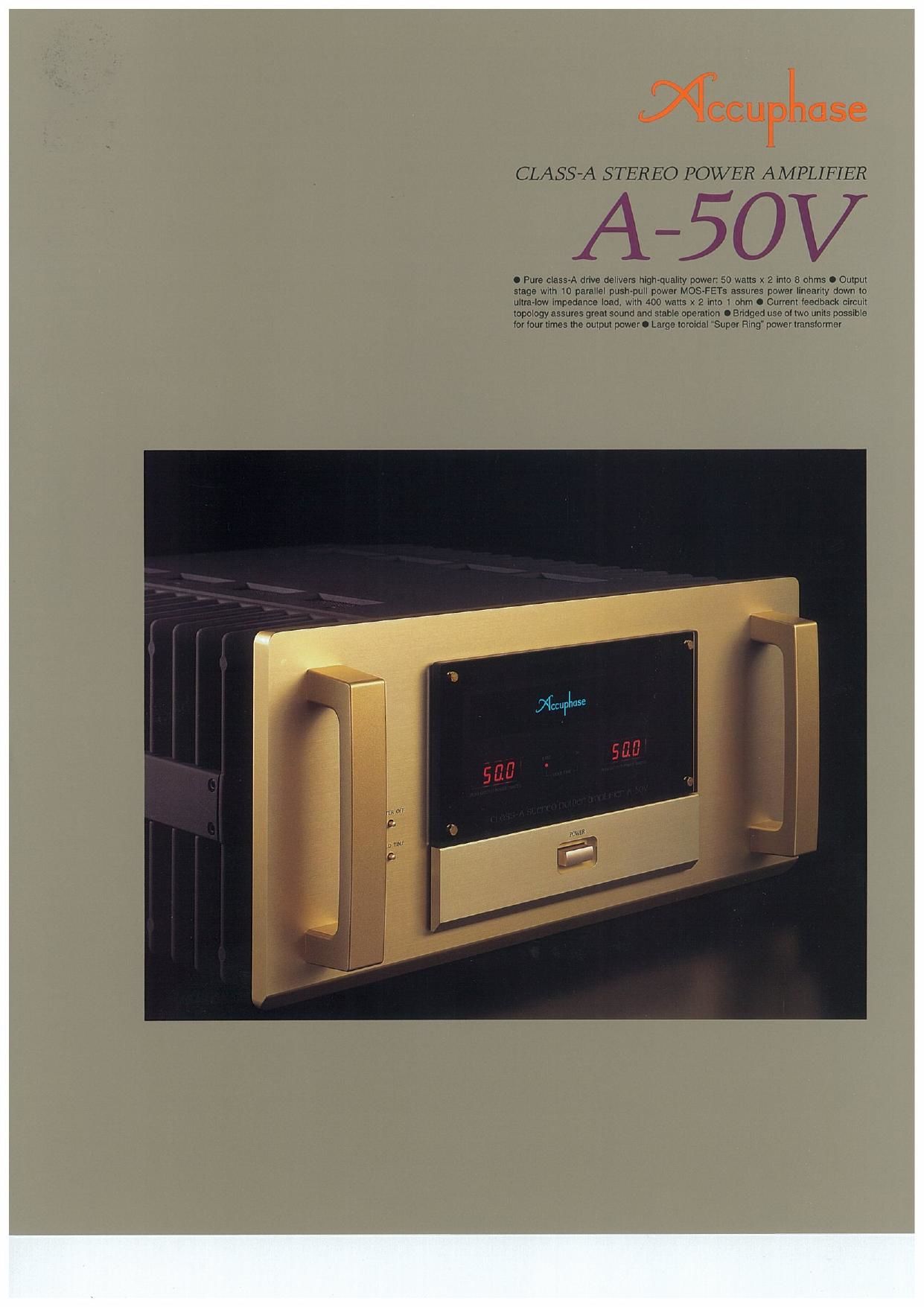
CLASS-A STEREO POWER AMPLIFIER
/\ /L / \ 7
/\f\ /,_J
/ W55)
H; 5N
a Pure class~A drive delwers high-quality power. so walls x 2 mm 9 ohms o Ou|pu|
stage wrln 10 parallel push-pull power MOS-PETS assures power lmearrly down lo
ullra-low lmpadanca load. wrlh 400 walls x 2 mm 1 ohm o Currem {eedback Clfliud
lopalogy assures greal sound and stable Dpelallon o Bridged use ol IWD umls possmle
lor lour limes me ourpur power 0 Large loroldal Super Fling" power Hanslormer
Page 2
The mono power amplifier M-2000 was widely
acclaimed as an impressive blend of perfor-
mance and sound quality thanks to the realiza-
tion of two major principles: very low output
impedance (Note 1), and constant drive volt-
age (Note 2).
The A-50V is a stereo power amplifier based
on the same design technology as the M2000.
It uses MOS-FET devices selected for their
musical qualities which are driven in a
no»holds-barred class-A circuit configuration.
The amplifier brings out even the most delicate
nuances in the source with full authorityThis is
Accuphase sound at its very best.
Pure class-A operation means that the circuit
always draws the same amount of power from
the power supply, regardless of the presence
or absence of a music signal. It is impervious
against external influences and has high sta-
bility. The output stage produces considerable
amounts of thermal energy, but in the A-SOV
this is dissipated by extravlarge heat sinks for
the left and right channels, to prevent the pos-
sibility of problems caused by internal heat
buildup.
Current feedback topology ensures good phase
characteristics in the upper frequency range,
combining operation stability with excellent fre-
quency responseThe MOS»FET devices in the
output stage are renowned for their high reli-
ability paired with favorable sonic properties.The
amplifier has outstanding power linearity real-
ized even at extremely low impedance loads,
as illustrated by the power rating that extends
from 50 watts into 8 ohms to 400 watts into 1
ohm. The muscle for this kind of performance
comes from an ultra-efficient Super Ring type
toroidal power transformer of massive propor-
tions, complemented by ample filtering capac-
ity.
Balanced inputs shut out externally induced
noise. Gold-plating of circuit traces, input/out-
put connectors, and all other major
signal-carrying parts ensures total sonic purity.
Bridged operation mode turns the unit into a
monaural amplifier with even more power.
Note 1: The reas
impedance
The load of a power amplifier, namely the loud-
speaker, generates a oounter-electromotive force
that can flow back into the amplifier via the NF loop.
This phenomenon is influenced by fluctuations in
speaker impedance, and interferes with the drive
performance of the amplifier.The output impedance
of a power amplifier should therefore be made as
low as possible by using output devices with high
current capability. This absorbs the counter-elec-
tromotive force generated by the voice coil and me
vents the occurrence of intermodulation distortion.
g for low amp output
Note 2: The constant drive voltage principle
Even in the presence of a load with wildly fluctuat-
ing impedance, the ideal power amplifier should
deliver a constant voltage signal to the load. When
the supplied voltage remains constant for any im-
pedance, output power will be inversely proportional
to the impedance of the load. A conventional am-
plifier can be easily made to operate in this way
down to a load impedance of about 4 ohms. At 1
ohm. however, eight times the output of an 8-ohm
load is called for, which can only be sustained by
an extremely well designed and capable output
stage and a highly robust and powerful power sup-
ply section.To build such an amplifier is ataskthat
requires not only considerable experience and re-
sources but also a thorough rethinking of basic prin-
ciples.
\-.-_-/
Power MOS-FET output stage in 10-parallel
push-pull configuration delivers 400 watts
into 1 ohm, 200 watts into 2 ohms,100 watts
into 4 ohms, or 50 watts into 8 ohms with
outstanding linearity
The output stage (Figure 1) uses power
MOS-FETs with negative thermal characteris-
tics. 10 pairs of these devices are arranged in a
,lll.\ FET-;
The peerless sound of pure class-A - Power MOS-FETS in the output stage
with a lO-parallel push-pull configuration perform extremely low output
impedance and realize constant-voltage drive for perfect speaker control.
Linear power progression ranges from 50 watts into 8 ohms to 400 watts into
1 ohm in stereo operation. Current feedback circuit topology assures great
sound and operation stability.
parallel push-pull configuration for each chan-
nel. The result is stable operation with ideal
power linearity even at ultra-low impedance load.
The maximum power dissipation of one
MOS-FET is 120 watts, but the actual power
load per pair is only 5 watts, so that each de-
vice is driven only in its low-power range where
linearity is excellent. The drive stage also uses
power MOS-FETs, in a cascade connection that
gives wide fre- z,
quency re-
sponse and re-
quires only 20
small amounts
of negative
feedback. This
also contrib-
utes to sound
quality.
Figure 2 shows
the output volt-
a g e/ c u r r e nt
characteristics
at various im-
pedance loads.
Output voltage
is almost con-
stant at various loads, which means that cur-
rent increases linearly.
Oumut current (A) -.
n
1152075wa
5
Output voltage (v) a...
Flgun 2 Low lmpodnnco in. output pow-v
(output von-g-Ioutput curt-ht)
Current feedback topology prevents phase
shifts
The amplifying circuits in the A-50V use the cur-
Currenl adder
IN
convonlr
Trim-Impedance
amplifier
Curr-m NFB
network
Flgura 3 Principle of current feedback amplifier
- Input Output
+ input
Buffer
rent feedback principle for negative feedback.
At the input point of the feedback loop, the im-
pedance is kept low and current
Ti:
0:
detection is performed. A
trans~impedance amplifier then con-
verts the current into a voltage to
ma:
be used as the feedback signal.
Since the impedance at the current
feedback point (current adder in Fig-
ure 3) is very low, there is almost no
3
'rr
phase shift. Phase compensation
therefore can be kept at a minimum.
0 A minimal amount of NFB results in
ourwr
assumes
8
'n'
-a:
Figure 1 Circuit diagram of amplifier section (one channel)
Figur- c mun-m mum. win. cumi man-cu
lmnmmmmnmmn